ADVFC32BH Analog Devices Inc, ADVFC32BH Datasheet - Page 6
ADVFC32BH
Manufacturer Part Number
ADVFC32BH
Description
IC CONV V/F F/V MONO TO100-10
Manufacturer
Analog Devices Inc
Type
Volt to Freq & Freq to Voltr
Datasheet
1.ADVFC32KNZ.pdf
(6 pages)
Specifications of ADVFC32BH
Rohs Status
RoHS non-compliant
Frequency - Max
500kHz
Full Scale
±100ppm/°C
Linearity
±0.05%
Mounting Type
Through Hole
Package / Case
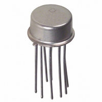
TO-100-10 Metal Can
Frequency
500kHz
Full Scale Range
0kHz To 500kHz
Linearity %
0.005%
Supply Voltage Range
± 9V To ± 18V
Digital Ic Case Style
TO-100
No. Of Pins
10
Msl
MSL 1 - Unlimited
Converter Function
VFC/FVC
Full Scale Frequency
500
Power Supply Requirement
Dual
Single Supply Voltage (typ)
Not RequiredV
Single Supply Voltage (max)
Not RequiredV
Single Supply Voltage (min)
Not RequiredV
Dual Supply Voltage (typ)
±15V
Dual Supply Voltage (min)
±9V
Dual Supply Voltage (max)
±18V
Operating Temperature (min)
-25C
Operating Temperature (max)
85C
Operating Temperature Classification
Commercial
Package Type
TO-100
Lead Free Status / Rohs Status
Not Compliant
Available stocks
Company
Part Number
Manufacturer
Quantity
Price


ADVFC32
The data link input voltage is changed in a frequency modulated
signal by the first ADVFC32. A 42.2 kΩ input resistor and a
100 kΩ offset resistor set the scaling so that a 0 V input signal
corresponds to 50 kHz, and a 10 V input results in the maximum
output frequency of 500 kHz. A high frequency optocoupler is
then used to transmit the signal across any common-mode volt-
age potentials to the receiving ADVFC32. The optocoupler is
not necessary in systems where common-mode noise is either
very small or a constant low level dc voltage. In systems where
common-mode voltage may present a problem, the connection
between the two locations should be through the optocoupler;
no power or ground connections need to be made.
The output of the optocoupler drives an ADVFC32 hooked up
in the F/V configuration. Since the reconstructed signal at Pin
10 has a considerable amount of carrier feedthrough, it is desir-
able to filter out any frequencies in the carrier range of 50 kHz
to 500 kHz. The frequency response of the F/V converter is only
3 kHz due to the pole made by the integrator, so a second 3 kHz
filter will not significantly limit the bandwidth. With the simple
one pole filter shown in Figure 6, the input to output 3 dB point
is approximately 2 kHz, and the output noise is less than 15 mV.
If a lower output impedance drive is needed, a two-pole active
filter is recommended as an output stage.
0.210 (5.33)
0.160 (4.06)
0.115 (2.93)
MAX
PIN 1
0.022 (0.558)
0.014 (0.356)
14
1
14-Lead Plastic DIP (N-14)
0.795 (20.19)
0.725 (18.42)
0.100 (2.54)
BSC
0.070 (1.77)
0.045 (1.15)
8
7
0.280 (7.11)
0.240 (6.10)
0.060 (1.52)
0.015 (0.38)
SEATING
PLANE
0.130
(3.30)
MIN
0.325 (8.25)
0.300 (7.62)
0.015 (0.381)
0.008 (0.204)
Dimensions shown in inches and (mm).
0.195 (4.95)
0.115 (2.93)
OUTLINE DIMENSIONS
Although the F/V conversion technique used in this circuit is
quite simple, it is also very limited in terms of its frequency
response and output ripple. The frequency response is limited
by the integrator time constant and while it is possible to decrease
that time constant, either signal range or output ripple must be
sacrificed. The performance of the circuit of Figure 6 is shown
in the photograph below. The top trace is the input signal, the
middle trace is the frequency-modulated signal at the opto-
coupler’s output, and the bottom trace is the recovered signal at
the output of the F/V converter.
0.040 (1.02) MAX
0.045 (1.14)
0.010 (0.25)
0.185 (4.70)
0.165 (4.19)
0.019 (0.48)
0.016 (0.41)
0.750 (19.05)
0.500 (12.70)
REFERENCE PLANE
BASE & SEATING PLANE
TO-100 (H-10A)
0.050 (1.27) MAX
0.021 (0.53)
0.016 (0.41)
0.250 (6.35) MIN
0.115
(2.92)
0.230 (5.84)
BSC
BSC
4
3
5
0.160 (4.06)
0.110 (2.79)
2
6
1
7
10
36° BSC
8
9
0.045 (1.14)
0.027 (0.69)
0.034 (0.86)
0.027 (0.69)
Related parts for ADVFC32BH
Image
Part Number
Description
Manufacturer
Datasheet
Request
R

Part Number:
Description:
±1.7g Dual-Axis IMEMS Accelerometer Evaluation Board
Manufacturer:
Analog Devices Inc
Datasheet:

Part Number:
Description:
Inertial Sensor Evaluation System
Manufacturer:
Analog Devices Inc
Datasheet:
Part Number:
Description:
Manufacturer:
Analog Devices Inc
Datasheet:
Part Number:
Description:
Manufacturer:
Analog Devices Inc
Datasheet:
Part Number:
Description:
Manufacturer:
Analog Devices Inc
Datasheet:
Part Number:
Description:
Manufacturer:
Analog Devices Inc
Datasheet:
Part Number:
Description:
Manufacturer:
Analog Devices Inc
Datasheet:
Part Number:
Description:
Manufacturer:
Analog Devices Inc
Datasheet:
Part Number:
Description:
Manufacturer:
Analog Devices Inc
Datasheet:
Part Number:
Description:
Manufacturer:
Analog Devices Inc
Datasheet:
Part Number:
Description:
Manufacturer:
Analog Devices Inc
Datasheet:
Part Number:
Description:
Manufacturer:
Analog Devices Inc
Datasheet:
Part Number:
Description:
Manufacturer:
Analog Devices Inc
Datasheet: