ADVFC32KN/+ Analog Devices Inc, ADVFC32KN/+ Datasheet
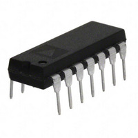
IC CONVERTER V/F-F/V 14DIP

ADVFC32KN/+

Manufacturer Part Number
ADVFC32KN/+
Description
IC CONVERTER V/F-F/V 14DIP
Manufacturer
Analog Devices Inc
Type
Volt to Freq & Freq to Voltr
Datasheet

Specifications of ADVFC32KN/+

Rohs Status
RoHS non-compliant
Frequency - Max
500kHz
Full Scale
±75ppm/°C
Linearity
±0.05%
Mounting Type
Through Hole
Package / Case
14-DIP (0.300", 7.62mm)
a
PRODUCT DESCRIPTION
The industry standard ADVFC32 is a low cost monolithic
voltage-to-frequency (V/F) converter or frequency-to-voltage
(F/V) converter with good linearity (0.01% max error at 10 kHz)
and operating frequency up to 0.5 MHz. In the V/F configuration,
positive or negative input voltages or currents can be converted
to a proportional frequency using only a few external compo-
nents. For F/V conversion, the same components are used with
a simple biasing network to accommodate a wide range of input
logic levels.
TTL or CMOS compatibility is achieved in the V/F operating
mode using an open collector frequency output. The pull-up
resistor can be connected to voltages up to 30 volts, or to 15 V
or 5 V for conventional CMOS or TTL logic levels. This resis-
tor should be chosen to limit current through the open collector
output to 8 mA. A larger resistance can be used if driving a high
impedance load.
Input offset drift is only 3 ppm of full scale per °C, and full-
scale calibration drift is held to a maximum of 100 ppm/°C
(ADVFC32BH) due to a low T.C. Zener diode.
The ADVFC32 is available in commercial, industrial, and
extended temperature grades. The commercial grade is pack-
aged in a 14-lead plastic DIP while the two wider temperature
range parts are packaged in hermetically sealed 10-lead cans.
PRODUCT HIGHLIGHTS
1. The ADVFC32 uses a charge balancing circuit technique
(see Functional Block Diagram) which is well suited to high
accuracy voltage-to-frequency conversion. The full-scale
operating frequency is determined by only one precision
resistor and capacitor. The tolerance of other support compo-
nents (including the integration capacitor) is not critical.
Inexpensive ± 20% resistors and capacitors can be used with-
out affecting linearity or temperature drift.
Frequency-to-Voltage Converter
2. The ADVFC32 is easily configured to satisfy a wide range of
3. The same components used for V/F conversion can also be
4. The ADVFC32 is intended as a pin-for-pin replacement for
5. The ADVFC32 is available in versions compliant with MIL-
system requirements. Input voltage scaling is set by selecting
the input resistor which sets the input current to 0.25 mA at
the maximum input voltage.
used for F/V conversion by adding a simple logic biasing
network and reconfiguring the ADVFC32.
VFC32 devices from other manufacturers.
STD-883. Refer to the Analog Devices Military Products
Databook or current ADVFC32/883B data sheet for detailed
specifications.
Voltage-to-Frequency and
PIN CONFIGURATION
H-10A Package
N-14 Package
(TOP VIEW)
ADVFC32

Related parts for ADVFC32KN/+

ADVFC32KN/+ Summary of contents

Page 1

PRODUCT DESCRIPTION The industry standard ADVFC32 is a low cost monolithic voltage-to-frequency (V/F) converter or frequency-to-voltage (F/V) converter with good linearity (0.01% max error at 10 kHz) and operating frequency up to 0.5 MHz. In the V/F configuration, positive ...

Page 2

ADVFC32–SPECIFICATIONS Model Min DYNAMIC PERFORMANCE Full-Scale Frequency Range 0 1 Nonlinearity kHz –0.01 MAX f = 100 kHz –0.05 MAX f = 0.5 MHz –0.20 MAX Full-Scale Calibration Error (Adjustable to Zero) vs. Supply (Full-Scale Frequency = ...

Page 3

UNIPOLAR V/F, POSITIVE INPUT VOLTAGE When operated as a V/F converter, the transformation from voltage to frequency is based on a comparison of input signal magnitude to the 1 mA internal current source. A more complete understanding of the ADVFC32 ...

Page 4

ADVFC32 Input resistance R is composed of a fixed resistor (R1) and a IN variable resistor (R3) to allow for initial gain error compensation. To cover all possible situations, R3 should be 20 This allows a ± ...

Page 5

Figure ppm/°C input resistor used with a 100 ppm/°C capacitor may result in a maximum overall circuit gain drift of: 100 ppm/°C (ADVFC32BH) + 100 ppm/°C (C1 ppm/° 210 ppm/°C ...

Page 6

ADVFC32 The data link input voltage is changed in a frequency modulated signal by the first ADVFC32. A 42.2 kΩ input resistor and a 100 kΩ offset resistor set the scaling so that input signal corresponds to ...

Related keywords