ADVFC32KN Analog Devices Inc, ADVFC32KN Datasheet
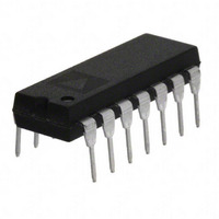
IC CONV V/F F/V 0-70DEGC 14-DIP

ADVFC32KN

Manufacturer Part Number
ADVFC32KN
Description
IC CONV V/F F/V 0-70DEGC 14-DIP
Manufacturer
Analog Devices Inc
Type
Volt to Freq & Freq to Voltr
Datasheet

Specifications of ADVFC32KN

Mounting Type
Through Hole
Rohs Status
RoHS non-compliant
Frequency - Max
500kHz
Full Scale
±75ppm/°C
Linearity
±0.05%
Package / Case
14-DIP (0.300", 7.62mm)
Frequency
0.5GHz
Linearity %
0.000005%
Digital Ic Case Style
DIP
No. Of Pins
14
Converter Type
Frequency/Voltage + Voltage/Frequency
Converter Function
VFC/FVC
Full Scale Frequency
500
Power Supply Requirement
Dual
Single Supply Voltage (typ)
Not RequiredV
Single Supply Voltage (max)
Not RequiredV
Single Supply Voltage (min)
Not RequiredV
Dual Supply Voltage (typ)
±15V
Dual Supply Voltage (min)
±9V
Dual Supply Voltage (max)
±18V
Operating Temperature (min)
0C
Operating Temperature (max)
70C
Operating Temperature Classification
Commercial
Package Type
PDIP
Lead Free Status / Rohs Status
Not Compliant

Available stocks

Company
Part Number
Manufacturer
Quantity
Price
Part Number:
ADVFC32KN
Manufacturer:
AD
Quantity:
5 510
Part Number:
ADVFC32KN
Manufacturer:
ADI
Quantity:
724
Part Number:
ADVFC32KN
Manufacturer:
ADI/亚德诺
Quantity:
20 000
Part Number:
ADVFC32KNZ
Manufacturer:
AD
Quantity:
450
Part Number:
ADVFC32KNZ
Manufacturer:
AD
Quantity:
27
Part Number:
ADVFC32KNZ
Quantity:
2 318
Part Number:
ADVFC32KNZ
Manufacturer:
ADI
Quantity:
724
Part Number:
ADVFC32KNZ
Manufacturer:
ADI/亚德诺
Quantity:
20 000
a
PRODUCT DESCRIPTION
The industry standard ADVFC32 is a low cost monolithic
voltage-to-frequency (V/F) converter or frequency-to-voltage
(F/V) converter with good linearity (0.01% max error at 10 kHz)
and operating frequency up to 0.5 MHz. In the V/F configuration,
positive or negative input voltages or currents can be converted
to a proportional frequency using only a few external compo-
nents. For F/V conversion, the same components are used with
a simple biasing network to accommodate a wide range of input
logic levels.
TTL or CMOS compatibility is achieved in the V/F operating
mode using an open collector frequency output. The pull-up
resistor can be connected to voltages up to 30 volts, or to 15 V
or 5 V for conventional CMOS or TTL logic levels. This resis-
tor should be chosen to limit current through the open collector
output to 8 mA. A larger resistance can be used if driving a high
impedance load.
Input offset drift is only 3 ppm of full scale per °C, and full-
scale calibration drift is held to a maximum of 100 ppm/°C
(ADVFC32BH) due to a low T.C. Zener diode.
The ADVFC32 is available in commercial, industrial, and
extended temperature grades. The commercial grade is pack-
aged in a 14-lead plastic DIP while the two wider temperature
range parts are packaged in hermetically sealed 10-lead cans.
PRODUCT HIGHLIGHTS
1. The ADVFC32 uses a charge balancing circuit technique
(see Functional Block Diagram) which is well suited to high
accuracy voltage-to-frequency conversion. The full-scale
operating frequency is determined by only one precision
resistor and capacitor. The tolerance of other support compo-
nents (including the integration capacitor) is not critical.
Inexpensive ± 20% resistors and capacitors can be used with-
out affecting linearity or temperature drift.
Frequency-to-Voltage Converter
2. The ADVFC32 is easily configured to satisfy a wide range of
3. The same components used for V/F conversion can also be
4. The ADVFC32 is intended as a pin-for-pin replacement for
5. The ADVFC32 is available in versions compliant with MIL-
system requirements. Input voltage scaling is set by selecting
the input resistor which sets the input current to 0.25 mA at
the maximum input voltage.
used for F/V conversion by adding a simple logic biasing
network and reconfiguring the ADVFC32.
VFC32 devices from other manufacturers.
STD-883. Refer to the Analog Devices Military Products
Databook or current ADVFC32/883B data sheet for detailed
specifications.
Voltage-to-Frequency and
PIN CONFIGURATION
H-10A Package
N-14 Package
(TOP VIEW)
ADVFC32

Related parts for ADVFC32KN

ADVFC32KN Summary of contents

Page 1

PRODUCT DESCRIPTION The industry standard ADVFC32 is a low cost monolithic voltage-to-frequency (V/F) converter or frequency-to-voltage (F/V) converter with good linearity (0.01% max error at 10 kHz) and operating frequency up to 0.5 MHz. In the V/F configuration, positive ...

Page 2

... ADVFC32KN ADVFC32BH 15 V unless otherwise noted.) ADVFC32S Max Min Typ Max 500 0 500 +0.01 –0.01 +0.01 +0.05 –0.05 +0.05 ± 0.05 +0.20 –0.20 +0.20 ± 5 +0.015 –0.015 +0.015 ...

Page 3

... V/F transfer function. Other component values and tem- perature coefficients are not critical. Table I. Suggested Values for Part 1 Number ADVFC32KN ADVFC32BH ADVFC32SH ) flows out of the IN NOTE 1 For details on grade and package offerings screened in accordance with MIL-STD-883, ) × This charge is refer to the Analog Devices Military Products Databook or current ADVFC32/883B OS data sheet.  ...

Page 4

ADVFC32 Input resistance R is composed of a fixed resistor (R1) and a IN variable resistor (R3) to allow for initial gain error compensation. To cover all possible situations, R3 should be 20 This allows a ± ...

Page 5

Figure ppm/°C input resistor used with a 100 ppm/°C capacitor may result in a maximum overall circuit gain drift of: 100 ppm/°C (ADVFC32BH) + 100 ppm/°C (C1 ppm/° 210 ppm/°C ...

Page 6

ADVFC32 The data link input voltage is changed in a frequency modulated signal by the first ADVFC32. A 42.2 kΩ input resistor and a 100 kΩ offset resistor set the scaling so that input signal corresponds to ...

Related keywords