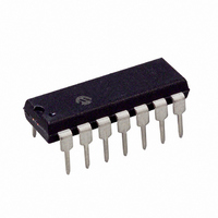
TC9401CPD Microchip Technology, TC9401CPD Datasheet - Page 15

TC9401CPD
Manufacturer Part Number
TC9401CPD
Description
IC V-FREQ/FREQ-V CONV 14DIP
Manufacturer
Microchip Technology
Type
Volt to Freq & Freq to Voltr
Datasheet
1.TC9402CPD.pdf
(28 pages)
Specifications of TC9401CPD
Frequency - Max
100kHz
Full Scale
±40ppm/°C
Linearity
±0.02%
Mounting Type
Through Hole
Package / Case
14-DIP (0.300", 7.62mm)
Primary Input Voltage
15V
No. Of Outputs
2
Voltage Regulator Case Style
DIP
No. Of Pins
14
Operating Temperature Range
0°C To +70°C
Svhc
No SVHC (15-Dec-2010)
Operating Temperature Max
70°C
Operating
RoHS Compliant
Supply Voltage (max)
15 V
Supply Voltage (min)
8 V
Maximum Operating Temperature
+ 70 C
Minimum Operating Temperature
0 C
Dual Supply Voltage
+/- 5 V
Full Scale Frequency
100 KHz
Linearity Error
+/- 0.08 % FSR
Maximum Dual Supply Voltage
+/- 7.5 V
Minimum Dual Supply Voltage
+/- 4 V
Mounting Style
Through Hole
Operating Supply Voltage
9 V, 12 V
Lead Free Status / RoHS Status
Lead free / RoHS Compliant
Lead Free Status / RoHS Status
Lead free / RoHS Compliant
Other names
158-1141
158-1141
158-1141
Available stocks
Company
Part Number
Manufacturer
Quantity
Price
Company:
Part Number:
TC9401CPD
Manufacturer:
Microchip Technology
Quantity:
135
Part Number:
TC9401CPD
Manufacturer:
MIC
Quantity:
20 000
FIGURE 6-2:
6.3
F
ever, these outputs may be useful for some applica-
tions, such as a buffer to feed additional circuitry. Then,
F
that F
will be square wave with a frequency of one-half F
FIGURE 6-3:
© 2007 Microchip Technology Inc.
OUT
OUT
OUT
and F
will follow the input frequency waveform, except
Input Buffer
Frequency
will go high 3 µs after F
OUT
Input
100 kΩ
Note:
/2 are not used in the F/V mode. How-
F/V Single Supply F/V Converter.
F/V Digital Outputs.
The output is referenced to Pin 6, which is at 6.2V (Vz). For frequency meter applications,
a 1 mA meter with a series scaling resistor can be placed across Pins 6 and 12.
Offset
Adjust
33 kΩ
0.5 ms
10 kΩ
F
6.2V
Min
IN
F
Input
OUT
0.01 µF
OUT
goes high; F
500 kΩ
/2
.01 µF
0.1 µF
IN914
OUT
OUT
/2
V+
Delay = 3 ms
10 kΩ
.
1.0 kΩ
1.0 kΩ
1.0
MΩ
11
5.0 ms
6
2
If these outputs are not used, Pins 8, 9 and 10 should be
connected to ground (see
Min
Zero
Adjust
I
GND
DET
BIAS
V+ = 10V to 15V
100 kΩ
TC9400
TC9400/9401/9402
V
V
REF
DD
V
14
7
REF
Amp Out
V
OUT
SS
GND
4
I
IN
5
3
12
6
Figure 6-3
1
MΩ
47 pF
.001 µF
DS21483D-page 15
and
V OUT
Figure
6-4).


