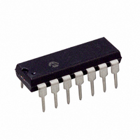
TC9400CPD Microchip Technology, TC9400CPD Datasheet - Page 6

TC9400CPD
Manufacturer Part Number
TC9400CPD
Description
IC V-FREQ/FREQ-V CONV 14DIP
Manufacturer
Microchip Technology
Type
Volt to Freq & Freq to Voltr
Specifications of TC9400CPD
Package / Case
14-DIP (0.300", 7.62mm)
Frequency - Max
100kHz
Full Scale
±40ppm/°C
Linearity
±0.05%
Mounting Type
Through Hole
Supply Voltage (max)
15 V
Supply Voltage (min)
8 V
Maximum Operating Temperature
70 C
Minimum Operating Temperature
0 C
Dual Supply Voltage
+/- 5 V
Full Scale Frequency
100 KHz
Linearity Error
+/- 0.25 % FSR
Maximum Dual Supply Voltage
+/- 7.5 V
Minimum Dual Supply Voltage
+/- 4 V
Mounting Style
Through Hole
Operating Supply Voltage
9 V or 12 V
Lead Free Status / RoHS Status
Lead free / RoHS Compliant
Lead Free Status / RoHS Status
Lead free / RoHS Compliant, Lead free / RoHS Compliant
Other names
158-1140
158-1140
158-1140
Available stocks
Company
Part Number
Manufacturer
Quantity
Price
Company:
Part Number:
TC9400CPD
Manufacturer:
MIT
Quantity:
6 234
Part Number:
TC9400CPD
Manufacturer:
TELCOM
Quantity:
20 000
TC9400/9401/9402
2.0
The descriptions of the pins are listed in
TABLE 2-1:
2.1
An external resistor, connected to V
point for the TC9400. Specifications for the TC9400 are
based on R
noted.
Increasing the maximum frequency of the TC9400
beyond 100 kHz is limited by the pulse width of the
pulse output (typically 3 µs). Reducing R
decrease the pulse width and increase the maximum
operating frequency, but linearity errors will also
increase. R
typically produce a maximum full scale frequency of
500 kHz.
2.2
This pin is the non-inverting input of the operational
amplifier. The low frequency set point is determined by
adjusting the voltage at this pin.
2.3
The inverting input of the operational amplifier and the
summing junction when connected in the V/F mode. An
input current of 10 μA is specified, but an over range
current up to 50 μA can be used without detrimental
effect to the circuit operation. I
junction of an operational amplifier. Voltage sources
cannot be attached directly, but must be buffered by
external resistors.
DS21483D-page 6
Pin No.
PIN DESCRIPTIONS
Bias Current (I
Zero Adjust
Input Current (I
10
12
13
14
11
1
2
3
4
5
6
7
8
9
BIAS
BIAS
can be reduced to 20 kΩ, which will
PIN FUNCTION TABLE
= 100 kΩ ±10%, unless otherwise
AMPLIFIER OUT Output of the integrator amplifier.
PULSE FREQ
THRESHOLD
FREQ/2 OUT
DETECTOR
ZERO ADJ
V
COMMON
OUTPUT
Symbol
REF
BIAS
GND
V
I
OUT
V
V
IN
BIAS
NC
IN
I
REF
IN
SS
DD
OUT
)
connects the summing
)
SS
, sets the bias
Table
This pin sets bias current in the TC9400. Connect to V
Low frequency adjustment input.
Input current connection for the V/F converter.
Negative power supply voltage connection, typically -5V.
Reference capacitor connection.
Analog ground.
Voltage reference input, typically -5V.
Frequency output. This open drain output will pulse LOW each time the Freq.
Threshold Detector limit is reached. The pulse rate is proportional to input voltage.
Source connection for the open drain output FETs.
This open drain output is a square wave at one-half the frequency of the pulse output
(Pin 8). Output transitions of this pin occur on the rising edge of Pin 8.
Input to the Threshold Detector. This pin is the frequency input during F/V operation.
No internal connection.
Positive power supply connection, typically +5V.
BIAS
2-1.
will
2.4
The charging current for C
pin. When the op amp output reaches the threshold
level, this pin is internally connected to the reference
voltage and a charge, equal to V
from the integrator capacitor. After about 3μsec, this pin
is internally connected to the summing junction of the
op amp to discharge C
ing ensures that the reference voltage is not directly
applied to the summing junction.
2.5
A reference voltage from either a precision source, or
the V
TC9400 is dependent on the voltage regulation and
temperature characteristics of the reference circuitry.
Since the TC9400 is a charge balancing V/F converter,
the reference current will be equal to the input current.
For this reason, the DC impedance of the reference
voltage source must be kept low enough to prevent
linearity errors. For linearity of 0.01%, a reference
impedance of 200Ω or less is recommended. A 0.1 µF
bypass capacitor should be connected from V
ground.
SS
supply is applied to this pin. Accuracy of the
Voltage Capacitor (V
Voltage Reference (V
Description
REF
© 2007 Microchip Technology Inc.
SS
. Break-before-make switch-
REF
through a 100 kΩ resistor.
is supplied through this
REF
REF
x C
REF
REF
Out)
)
, is removed
REF
to


