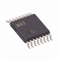
MAX6698UE38+ Maxim Integrated Products, MAX6698UE38+ Datasheet - Page 10

MAX6698UE38+
Manufacturer Part Number
MAX6698UE38+
Description
IC TEMP MONITOR 7CH 16-TSSOP
Manufacturer
Maxim Integrated Products
Datasheet
1.MAX6698EE99.pdf
(24 pages)
Specifications of MAX6698UE38+
Function
Temp Monitoring System (Sensor)
Topology
ADC, Buffer, Multiplexer, Register Bank
Sensor Type
External & Internal
Sensing Temperature
-40°C ~ 125°C, External Sensor
Output Type
I²C™/SMBus™
Output Alarm
Yes
Output Fan
Yes
Voltage - Supply
3 V ~ 5.5 V
Operating Temperature
-40°C ~ 125°C
Mounting Type
Surface Mount
Package / Case
16-TSSOP
Full Temp Accuracy
+/- 3.5 C, +/- 3 C
Digital Output - Bus Interface
Serial (2-Wire)
Digital Output - Number Of Bits
11 bit
Maximum Operating Temperature
+ 125 C
Minimum Operating Temperature
- 40 C
Lead Free Status / RoHS Status
Lead free / RoHS Compliant
An ALERT interrupt occurs when the internal or external
temperature reading exceeds a high-temperature limit
(user programmable). The ALERT interrupt output sig-
nal can be cleared by reading the status register(s)
associated with the fault(s) or by successfully respond-
ing to an alert response address transmission by the
master. In both cases, the alert is cleared but is
reasserted at the end of the next conversion if the fault
condition still exists. The interrupt does not halt auto-
matic conversions. The ALERT output is open drain so
that multiple devices can share a common interrupt
line. All ALERT interrupts can be masked using the
configuration 3 register. The POR state of these regis-
ters is shown in Table 4.
The SMBus alert response interrupt pointer provides
quick fault identification for simple slave devices that
lack the complex logic needed to be a bus master.
Upon receiving an interrupt signal, the host master can
broadcast a receive byte transmission to the alert
response slave address (see the Slave Addresses sec-
tion). Then, any slave device that generated an inter-
rupt attempts to identify itself by putting its own
address on the bus.
The alert response can activate several different slave
devices simultaneously, similar to the I
If more than one slave attempts to respond, bus arbitra-
tion rules apply, and the device with the lower address
code wins. The losing device does not generate an
acknowledgment and continues to hold the ALERT line
low until cleared. (The conditions for clearing an alert
vary depending on the type of slave device.)
Successful completion of the alert response protocol
clears the output latch. If the condition that caused the
alert still exists, the MAX6698 reasserts the ALERT
interrupt at the end of the next conversion.
The MAX6698 has four overtemperature registers that
store remote alarm threshold data for the OVERT out-
put. OVERT is asserted when a channel’s measured
temperature (voltage in the case of the thermistor chan-
nels) is greater than the value stored in the correspond-
ing threshold register. OVERT remains asserted until
the temperature drops below the programmed thresh-
old minus 4°C hysteresis for remote-diode channel 1, or
7-Channel Precision Remote-Diode, Thermistor,
and Local Temperature Monitor
10
______________________________________________________________________________________
OVERT Overtemperature Alarms
ALERT Response Address
ALERT Interrupt Mode
2
C General Call.
4 LSB hysteresis for thermistor channels 1, 2, and 3. An
overtemperature output can be used to activate a cool-
ing fan, send a warning, initiate clock throttling, or trig-
ger a system shutdown to prevent component damage.
See Table 4 for the POR state of the overtemperature
threshold registers.
The 8-bit command byte register (Table 4) is the master
index that points to the various other registers within the
MAX6698. This register’s POR state is 0000 0000.
There are three read-write configuration registers
(Tables 5, 6, 7) that can be used to control the
MAX6698’s operation.
The configuration 1 register (Table 5) has several func-
tions. Bit 7(MSB) is used to put the MAX6698 either in
software standby mode (STOP) or continuous conver-
sion mode. Bit 6 resets all registers to their power-on
reset conditions and then clears itself. Bit 5 disables
the SMBus timeout. Bit 4 enables more frequent con-
versions on channel 1, as described in the ADC
Conversion Sequence section. Bit 3 enables resistance
cancellation on channel 1. See the Series Resistance
Cancellation section for more details. The remaining
bits of the configuration 1 register are not used. The
POR state of this register is 0000 0000 (00h).
The configuration 2 register functions are described in
Table 6. Bits [6:0] are used to mask the ALERT interrupt
output. Bit 6 masks the local alert interrupt, bits 5
through 3 mask the remote-diode ALERT interrupts, and
bits 2 through 0 mask the thermistor alert interrupts. The
power-up state of this register is 0000 0000 (00h).
Table 7 describes the configuration 3 register. Bits 5, 4,
3, and 0 mask the OVERT interrupt output for thermistor
channels 1, 2, and 3 and remote-diode channel 1. The
remaining bits, 7, 6, 2, and 1, are reserved. The power-
up state of this register is 0000 0000 (00h).
Configuration Bytes Functions
Command Byte Functions
Configuration 1 Register
Configuration 2 Register
Configuration 3 Register


