AD636KH Analog Devices Inc, AD636KH Datasheet - Page 10
AD636KH
Manufacturer Part Number
AD636KH
Description
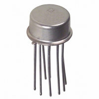
IC CONV RMS-DC LOW LVL TO100-10
Manufacturer
Analog Devices Inc
Datasheet
1.AD636JDZ.pdf
(16 pages)
Specifications of AD636KH
Rohs Status
RoHS non-compliant
Current - Supply
800µA
Voltage - Supply
±2.5 V ~ 16 V
Mounting Type
Through Hole
Package / Case
TO-100, Metal Can (10 Leads)
Available stocks
Company
Part Number
Manufacturer
Quantity
Price


AD636
swing, this configuration allows the output to swing fully down
to ground in single-supply applications without the problems
associated with most IC operational amplifiers.
When this amplifier is used in dual-supply applications as an
input buffer amplifier driving a load resistance referred to
ground, steps must be taken to ensure an adequate negative
voltage swing. For negative outputs, current flows from the load
resistor through the 40 kΩ emitter resistor, setting up a voltage
divider between −V
limits the available negative output swing of the buffer. The
addition of an external resistor in parallel with R
voltage divider such that increased negative swing is possible.
Figure 14 shows the value of R
V
R
by an amount equal to R
current with no R
FREQUENCY RESPONSE
The AD636 uses a logarithmic circuit to perform the implicit
rms computation. As with any log circuit, bandwidth is
proportional to signal level. The solid lines in Figure 15
represent the frequency response of the AD636 at input levels
from 1 mV to 1 V rms. The dashed lines indicate the upper
frequency limits for 1%, 10%, and ±3 dB of reading additional
EXTERNAL
PEAK
to −V
1.0
0.5
BUFFER
0
Figure 14. Ratio of Peak Negative Swing to −V
0
INPUT
Figure 13. AD636 Buffer Amplifier Simplified Schematic
increases the quiescent current of the buffer amplifier
S
for several values of R
EXTERNAL
S
1k
for Several Load Resistances
and ground. This reduced effective −V
5µA
CURRENT
MIRROR
+V
EXT
is 30 μA at −V
S
5µA
/−V
R
EXTERNAL
–V
EXTERNAL
S
S
10k
. Nominal buffer quiescent
(OPTIONAL, SEE TEXT)
10kΩ
R
40kΩ
L
LOAD
R
= 6.7kΩ
(Ω)
E
R
for a particular ratio of
EXTERNAL
. The addition of
BUFFER
OUTPUT
S
= −5 V.
R
R
100k
L
L
= 16.7kΩ
= 50kΩ
S
vs. R
E
R
alters this
LOAD
EXTERNAL
1M
S
Rev. D | Page 10 of 16
,
error. For example, note that a 1 V rms signal produces less than
1% of reading additional error up to 220 kHz. A 10 mV signal
can be measured with 1% of reading additional error (100 μV)
up to 14 kHz.
AC MEASUREMENT ACCURACY AND CREST
FACTOR (CF)
Crest factor is often overlooked in determining the accuracy of
an ac measurement. Crest factor is defined as the ratio of the
peak signal amplitude to the rms value of the signal (CF = V
rms). Most common waveforms, such as sine and triangle
waves, have relatively low crest factors (<2). Waveforms that
resemble low duty cycle pulse trains, such as those occurring in
switching power supplies and SCR circuits, have high crest
factors. For example, a rectangular pulse train with a 1% duty
cycle has a crest factor of 10 (CF = 1/√ η ).
Figure 16 is a curve of reading error for the AD636 for a
200 mV rms input signal with crest factors from 1 to 7. A
rectangular pulse train (pulse width 200 μs) was used for this
test because it is the worst-case waveform for rms measurement
(all the energy is contained in the peaks). The duty cycle and
peak amplitude were varied to produce crest factors from 1 to 7
while maintaining a constant 200 mV rms input amplitude.
200m
100m
0.1m
30m
10m
–0.5
–1.0
1m
0.5
1
0
1k
1
1V rms INPUT
200mV rms INPUT
100mV rms INPUT
1mV rms INPUT
30mV rms INPUT
10mV rms
INPUT
0
V
P
Figure 15. AD636 Frequency Response
200µs
2
Figure 16. Error vs. Crest Factor
10k
T
E
3
O
FREQUENCY (Hz)
CREST FACTOR
100k
4
1%
CF = 1/
E
ŋ
IN
= DUTY CYCLE =
(rms) = 200mV
5
10%
ŋ
1M
±3dB
6
200µs
T
10M
7
P
/V
Related parts for AD636KH
Image
Part Number
Description
Manufacturer
Datasheet
Request
R

Part Number:
Description:
±1.7g Dual-Axis IMEMS Accelerometer Evaluation Board
Manufacturer:
Analog Devices Inc
Datasheet:

Part Number:
Description:
Inertial Sensor Evaluation System
Manufacturer:
Analog Devices Inc
Datasheet:
Part Number:
Description:
Manufacturer:
Analog Devices Inc
Datasheet:
Part Number:
Description:
Manufacturer:
Analog Devices Inc
Datasheet:
Part Number:
Description:
Manufacturer:
Analog Devices Inc
Datasheet:
Part Number:
Description:
Manufacturer:
Analog Devices Inc
Datasheet:
Part Number:
Description:
Manufacturer:
Analog Devices Inc
Datasheet:
Part Number:
Description:
Manufacturer:
Analog Devices Inc
Datasheet:
Part Number:
Description:
Manufacturer:
Analog Devices Inc
Datasheet:
Part Number:
Description:
Manufacturer:
Analog Devices Inc
Datasheet:
Part Number:
Description:
Manufacturer:
Analog Devices Inc
Datasheet:
Part Number:
Description:
Manufacturer:
Analog Devices Inc
Datasheet:
Part Number:
Description:
Manufacturer:
Analog Devices Inc
Datasheet: