NCP349MNAETBG ON Semiconductor, NCP349MNAETBG Datasheet - Page 10
NCP349MNAETBG
Manufacturer Part Number
NCP349MNAETBG
Description
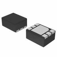
IC CTLR OVP 28V W/NMOS 6-DFN
Manufacturer
ON Semiconductor
Datasheet
1.NCP349MNBGTBG.pdf
(12 pages)
Specifications of NCP349MNAETBG
Applications
Overvoltage Protection Controller
Voltage - Supply
1.2 V ~ 28 V
Current - Supply
70µA
Operating Temperature
-40°C ~ 85°C
Mounting Type
Surface Mount
Package / Case
6-VFDFN Exposed Pad
Operating Temperature (max)
85C
Operating Temperature (min)
-40C
Pin Count
6
Mounting
Surface Mount
Package Type
DFN EP
Screening Level
Industrial
Lead Free Status / RoHS Status
Lead free / RoHS Compliant
Voltage - Input
-
Lead Free Status / Rohs Status
Lead free / RoHS Compliant
Available stocks
Company
Part Number
Manufacturer
Quantity
Price


Undervoltage Lockout (UVLO)
device has a built−in undervoltage lockout (UVLO) circuit.
During V
disconnected from input until V
plus hysteresis, nominal. The FLAG output is tied to low as
long as V
a built−in hysteresis to provide noise immunity to transient
condition. Additional UVLO thresholds ranging from
UVLO can be manufactured. Contact your ON
Semiconductor representative for availability.
Overvoltage Lockout (OVLO)
overvoltage, the device has a built−in overvoltage lockout
(OVLO) circuit. During overvoltage condition, the output
remains disabled as long as the input voltage exceeds
typical OVLO. Additional OVLO thresholds ranging from
OVLO can be manufactured. Contact your ON
Semiconductor representative for availability.
This circuit has a built−in hysteresis to provide noise
immunity to transient
FLAG Output
external systems that a fault has occurred.
exceeded or when the V
threshold. When V
FLAG is held high, keeping in mind that an additional t
delay has been added between available output and FLAG
= high. The pin is an open drain output, thus a pull up
resistor (typically 1 MW, minimum 10 kW) must be added
to V
level will always reflects V
turned off (EN = 1).
EN Input
to low or connected to ground. A high level on the pin,
disconnects OUT pin from IN pin. EN does not overdrive
an OVLO or UVLO fault.
Internal NMOS FET
FET to protect the systems, connected on OUT pin, from
positive overvoltage. Regarding electrical characteristics,
the R
on V
As example: R
Typical R
V
NMOS losses = R
out
To ensure proper operation under any conditions, the
To protect connected systems on V
FLAG output is tied to low until V
The NCP349 provides a FLAG output, which alerts
This pin is tied to low as soon the OVLO threshold is
To enable normal operation, the EN pin shall be forced
The NCP349 includes an internal Low R
bat
out
= 8 x 0.618 = 4.95 V
DS(on)
. Minimum V
pin.
in
DS(on)
in
, during normal operation, will create low losses
does not reach UVLO threshold. This circuit has
positive going slope, the output remains
load
= 65 mW, I
DS(on)
= 8.0 W, V
in
bat
conditions.
level recovers normal condition,
supply must be 2.5 V. The FLAG
x Iout
in
out
in
in
2
level is below the UVLO
status, even if the device is
= 618 mA
= 0.065 x 0.618
in
= 5.0 V
voltage is below UVLO,
in
is higher than OVLO.
out
DS(on)
2
pin from
= 25 mW
NMOS
http://onsemi.com
start
10
ESD Tests
1.0 mF (minimum) must be connected between V
GND, close to the device.
protected input. In Contact condition, V
ESD protected input.
electrostatic discharge waveform.
PCB Recommendations
PCB rules must be respected to properly evacuate the heat
out of the silicon. The pin 7 (exposed pad) is internally
connected to the internal NMOS Drain (Input). This
exposed pad must be used to increase heat transfer and must
be connected to Pin 1. Of course, in any case, this pad
shall be not connected to any other potential.
200
180
160
140
120
100
The NCP349 input pin fully supports the IEC61000−4−2.
That means, in Air condition, V
Please refer to Figure 19 to see the IEC 61000−4−2
The NCP349 integrates a 2 A rated NMOSFET, and the
80
60
0
Figure 19. Electrostatic Discharge Waveform
100
Copper heat spreader area (mm^2)
Theta JA curve with PCB cu thk 1.0 oz
Theta JA curve with PCB cu thk 2.0 oz
Power curve with PCB cu thk 2.0 oz
Power curve with PCB cu thk 1.0 oz
200
Figure 20.
300
400
in
has a "15 kV ESD
500
in
has "8.0 kV
600
700
in
1.75
1.5
1.25
1
0.75
0.5
0.25
and
Related parts for NCP349MNAETBG
Image
Part Number
Description
Manufacturer
Datasheet
Request
R

Part Number:
Description:
ON Semiconductor [VOLTAGE REGULATOR]
Manufacturer:
ON Semiconductor
Datasheet:
Part Number:
Description:
357-036-542-201 CARDEDGE 36POS DL .156 BLK LOPRO
Manufacturer:
ON Semiconductor
Datasheet:
Part Number:
Description:
357-036-542-201 CARDEDGE 36POS DL .156 BLK LOPRO
Manufacturer:
ON Semiconductor
Datasheet:
Part Number:
Description:
357-036-542-201 CARDEDGE 36POS DL .156 BLK LOPRO
Manufacturer:
ON Semiconductor
Datasheet:
Part Number:
Description:
357-036-542-201 CARDEDGE 36POS DL .156 BLK LOPRO
Manufacturer:
ON Semiconductor
Datasheet:
Part Number:
Description:
357-036-542-201 CARDEDGE 36POS DL .156 BLK LOPRO
Manufacturer:
ON Semiconductor
Datasheet:
Part Number:
Description:
357-036-542-201 CARDEDGE 36POS DL .156 BLK LOPRO
Manufacturer:
ON Semiconductor
Datasheet:
Part Number:
Description:
357-036-542-201 CARDEDGE 36POS DL .156 BLK LOPRO
Manufacturer:
ON Semiconductor
Datasheet:
Part Number:
Description:
357-036-542-201 CARDEDGE 36POS DL .156 BLK LOPRO
Manufacturer:
ON Semiconductor
Datasheet:
Part Number:
Description:
357-036-542-201 CARDEDGE 36POS DL .156 BLK LOPRO
Manufacturer:
ON Semiconductor
Datasheet:
Part Number:
Description:
357-036-542-201 CARDEDGE 36POS DL .156 BLK LOPRO
Manufacturer:
ON Semiconductor
Datasheet:
Part Number:
Description:
Manufacturer:
ON Semiconductor
Datasheet:
Part Number:
Description:
Manufacturer:
ON Semiconductor
Datasheet:
Part Number:
Description:
Manufacturer:
ON Semiconductor
Datasheet: