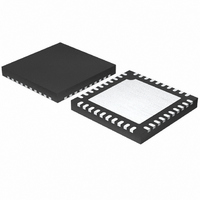
MAX8784ETL+ Maxim Integrated Products, MAX8784ETL+ Datasheet - Page 18

MAX8784ETL+
Manufacturer Part Number
MAX8784ETL+
Description
IC REG STP UP W/AMP 40-TQFN
Manufacturer
Maxim Integrated Products
Datasheet
1.MAX8784ETL.pdf
(24 pages)
Specifications of MAX8784ETL+
Applications
LCD TV/Monitor
Voltage - Supply
4 V ~ 5.5 V
Operating Temperature
-40°C ~ 85°C
Mounting Type
Surface Mount
Package / Case
40-TQFN Exposed Pad
Operating Supply Voltage
4 V to 5.5 V
Maximum Operating Temperature
- 40 C
Mounting Style
SMD/SMT
Maximum Power Dissipation
2857 mW
Minimum Operating Temperature
+ 85 C
Supply Current
4 mA
Lead Free Status / RoHS Status
Lead free / RoHS Compliant
Current - Supply
-
Lead Free Status / Rohs Status
Lead free / RoHS Compliant
HVS mode is designed as a special operating mode for
end-of-line panel testing. In HVS mode, higher than
normal voltages are forced to the power-supply outputs
to expose faults in the LCD panel. HVS pin is forced
logic-high to enable HVS mode. In HVS mode opera-
tion, FBP is ignored and the positive charge-pump reg-
ulates to a fixed-output voltage of 30V. To raise the
step-up regulator output voltage in HVS operation, the
Step-Up Regulator, Internal Charge Pumps, Switch
Control, and Operational Amplifier for TFT LCDs
Figure
18
______________________________________________________________________________________
-9V, 20mA
7. HVS Mode Operation
VGOFF
VIN = 5V
10µF
AVDD
102kΩ
11kΩ
10kΩ
10kΩ
1µF
VCOM
VCOM
VCOM
0.22µF
VIN
1µF
C4
V
POS3
OUT3
POS1
NEG1
OUT1
POS2
NEG2
OUT2
HVS
AGND
FBN
PGND
REF
DRVN
CC
AVDD
SUP
10µF
HVS Mode
0.1µF 0.1µF
MAX8784
C1N
C1P
10µF
C2N
0.1µF
open-drain RSET pin is pulled to GND. In Figure 1, resis-
tor R8 becomes parallel to R10, which reduces the feed-
back resistance during HVS operation. This special
feature allows the customer to select a resistor that sets
an appropriate HVS voltage according to the panel
requirements. The negative charge pump operates nor-
mally. Figure 7 shows the typical application circuit in
HVS mode.
3µH
C2P
COMP
PGND
SHDN
GDEL
POUT
ADEL
RSET
GON
DRN
CTL
FBP
LX
FB
V
POUT
100kΩ
FROM TCON
FROM SYSTEM
FBP IGNORED
432kΩ
20kΩ
= 30V
0.1µF
330pF
1µF
82kΩ
RSET = LOW
AVDD
0.01µF
10µF
VGON
30V, 20mA
205kΩ
20kΩ
10µF
AVDD
17V, 0.65A


