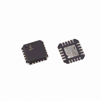
ISL6271ACRZ-T Intersil, ISL6271ACRZ-T Datasheet - Page 7

ISL6271ACRZ-T
Manufacturer Part Number
ISL6271ACRZ-T
Description
IC PMIC XSCALE REG 20-QFN
Manufacturer
Intersil
Datasheet
1.ISL6271ACRZ-T.pdf
(16 pages)
Specifications of ISL6271ACRZ-T
Applications
Processor
Current - Supply
380µA
Voltage - Supply
2.76 V ~ 5.5 V
Operating Temperature
-25°C ~ 85°C
Mounting Type
Surface Mount
Package / Case
20-QFN
Rohs Compliant
Yes
Lead Free Status / RoHS Status
Lead free / RoHS Compliant
Other names
ISL6271ACRZ-TTR
Available stocks
Company
Part Number
Manufacturer
Quantity
Price
Part Number:
ISL6271ACRZ-T
Manufacturer:
INTERSIL
Quantity:
20 000
Typical Operating Performance
Test results from the Intersil ISL6271A Customer Reference Board (CRB). Output filter on switcher made up of a 4.7µH drumcore with 100mΩ of
DCR and an output capacitance of 10µF. X5R; Rcomp = 50kΩ, Vin = 3.6V unless otherwise noted.
Forced PGOOD fault. Converter operating in CCM at 420mA prior to
Functional Pin Description
PVCC - Input power to the core switching regulator. This
voltage is typically supplied by a the primary, single-cell
Li-ion battery or power adapter.
VCC. Voltage source for control circuitry. Must be held within
0.3V of PVCC.
BBAT. Secondary back-up voltage used to provide an
indication of the main battery status when the main battery is
low or absent. BBAT is typically a coin cell device and must
be maintained between 1.5V and 3.75V if it is not connected
to VCC pin. Connect it to VCC if BFLT# function is not used.
PHASE. The output switching node that connects to the
output inductor to generate the processor core voltage.
VOUT. Output voltage of the core regulator. Programmable
from 0.85 to 1.6V via the integrated I
LVCC. Input voltage to the VSRAM and VPLL LDO pass
elements. To minimize power loss across the pass element
this should be tied to a pre-regulated system voltage
between 1.8V and 2.5V. LVCC can operate from the main
battery input when lower voltages are unavailable.
VPLL. 1.3V LDO regulator designed to supply power to the
phase-locked loop circuitry internal to the microprocessor.
VSRAM. 1.1V LDO regulator designed to supply power to
the microprocessor SRAM circuitry.
FB. Core voltage feedback (to the error amplifier) via an
external compensation resistor.
SOFT. An external capacitor connected between this pin and
ground controls the regulators output rise time. The start-up
ramp begins when VCC reaches its power-on-reset (POR)
rising threshold and the EN pin is high.
applying a 320mA transient step. This pushes the regulator beyond
the overcurrent threshold of 700mA. The phase node three-stated
FIGURE 14. FORCED PGOOD FAULT
and follows Vout to 0V. 20µs/DIV
PHASE
PGOOD
7
VOUT
2
C bus or VID pins.
(Continued)
ISL6271A
EN - The ISL6271A outputs are enabled when a voltage
greater than 2V is applied to the EN pin. The core regulator
output MOSFETs bridge is turned off and the LDOs are
disabled when EN is pulled low.
BFLT# - Battery fault indicator. A high level indicates the
adequacy of the battery for regulator start-up. Designed to
interface with the processor General Purpose IO, this pin is
actively pulled low when the main battery is absent.
PGOOD - An open-drain output that indicates the status of
the three regulators. It is pulled low when any of the regulators
are outside their voltage tolerances.
VIDEN - Pull this pin low to enable I
Connecting this pin to VCC disables the I
enables the VID inputs. In this mode the slew rate is fixed at
a value determined by the soft-start capacitor.
SCL (VID0) - This is a dual function pin. When VIDEN is low
it acts as the I
pin acts as bit 0 to the VID DAC.
SDA (VID1) - This is a dual function pin. When VIDEN is low
it acts as the I
voltage level and slew rate instructions to the ISL6271A.
When VIDEN is high this pin acts as bit 1 to the VID DAC.
VID2, VID3 - VID inputs to the error amplifier reference DAC.
Used to control the core voltage when VIDEN is high.
GND - Device signal ground. Connected to PGND at a
single point to avoid ground loops.
PGND - Power ground return connection for the internal
synchronous rectifier.
EN
Vout = 0.85V prior to EN going low, 400ns/DIV
2
PGOOD delay = 186ns from disable.
2
C clock input (SCL). When VIDEN is high this
C data/address line (SDA) used to transfer
FIGURE 15. PGOOD DELAY
PHASE
PGOOD
VOUT
2
C communication.
2
C bus and
FN9171.1


