FPF2025 Fairchild Semiconductor, FPF2025 Datasheet - Page 14
FPF2025
Manufacturer Part Number
FPF2025
Description
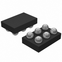
IC LOAD SWITCH 100MA 6-WLCSP
Manufacturer
Fairchild Semiconductor
Type
High Side Switchr
Datasheet
1.FPF2026.pdf
(17 pages)
Specifications of FPF2025
Number Of Outputs
1
Rds (on)
315 mOhm
Internal Switch(s)
Yes
Current Limit
150mA
Voltage - Input
1.6 ~ 5.5 V
Operating Temperature
-40°C ~ 85°C
Mounting Type
Surface Mount
Package / Case
6-WLCSP
Lead Free Status / RoHS Status
Lead free / RoHS Compliant


©2008 Fairchild Semiconductor Corporation
FPF2024/5/6/7 Final. B
P
Output of FPF2027 is shorted to GND.
P
Application Information
Input Capacitor
To limit the voltage drop on the input supply caused by transient
in-rush currents when the switch is turned on into a discharged
load capacitor or a short-circuit, a capacitor is recommended to
be placed between V
series feature a slow turn-on to limit the inrush current and
requires a smaller input capacitor. A 1uF ceramic capacitor, C
placed close to the pins is typically sufficient. Higher values of
C
Output Capacitor
A 0.1uF capacitor C
GND. This capacitor will prevent parasitic board inductances
from forcing V
FPF2024, FPF2025 and FPF2026, the total output capacitance
needs to be kept below a maximum value, C
the part from registering an over-current condition beyond the
Blanking Time and turning-off the switch. The maximum output
capacitance can be determined from the following formula:
Power Dissipation
During normal operation as a switch, the power dissipation is
small and has little effect on the operating temperature of the
part. The maximum power dissipation while switch is in normal
operation occurs just before a part enters the current limit. This
may be calculated using the formula bellow:
If the part goes into current limit, the maximum power
dissipation occurs when the output of switch is shorted to
ground. For the FPF2024 and FPF2025, the power dissipation
will scale with the Auto-Restart Time, t
Current Blanking Time, t
dissipated for the FPF2024 and FPF2025 is:
Take note that this is below the maximum package power
dissipation, and the thermal shutdown feature protection
provides additional safety to protect the part from damage due
to excessive heating. The junction temperature is only able to
increase to the thermal shutdown threshold. Once this
temperature has been reached, toggling ON will have no affect
until the junction temperature drops below the thermal
shutdown exit temperature. For the FPF2027, a short on the
output will cause the part to operate in a constant current state
dissipating a worst case power of:
This power dissipation is significant enough that it will activate
the thermal shutdown protection, and the part will cycle in and
out of thermal shutdown so long as the ON pin is active and the
output short is present.
P
Max
Max(Normal Operation)
IN
Max(Current limit)
can be used to further reduce the voltage drop.
= V
IN(Max)
OUT
C
X I
OUT(Max)
=
=
below GND when the switch turns-off. For the
LIM(Max)
OUT
= (I
= (0.2)
t
BLANK
10 + 70
IN
LIM(Max)
BLANK
, should be placed between V
10
=
t
and GND. The FPF2024-FPF2027
= 5.5X0.2 =1.1 W
BLANK
2
x 0.58 = 23.2 mW, for V
+ t
. In this case the maximum power
I
)
LIM(Max)
2
RSTRT
x 5.5 x 0.2 =137 mW
x R
ON(Max)
V
x t
IN
RSTRT
BLANK(Min)
x V
OUT(max)
IN(Max)
, and the Over
, to prevent
x I
IN
OUT
=1.6V
LIM(Max)
and
IN
,
14
Improving Thermal Performance
An improper layout could result in higher junction temperature
and ultimately trigger the thermal shutdown protection feature.
This concern applies particularly significant for the FPF2027
where the switch is in constant current mode in the overload
conditions.
The following techniques have been identified to improve the
thermal performance of this family of devices. These techniques
are listed in order of the significance of their impact.
FPF202X Demo Board
FPF202X Demo board has components and circuitry to
demonstrate the functions and features of the FPF202X load
switch family. An N-Channel MOSFET(Q), in series with a 7.5Ω
resistor, are connected between V
device. By turning on the Q transistor, the 7.5Ω is loaded to the
output voltage and simulates an over-current condition. The R2
resistor is connected between FLAGB pin and input voltage as
pull-up resistor for FPF2024, FPF2026 and FPF2027 devices.
The FPF2025 does not require a pull-up resistor due to its
CMOS output structure.
The thermal performance of the board is improved using the
techniques recommended in the layout recommendations
section of datasheet.
NC pin can be connected to the GND plane to improve
thermal performance.
The V
generated during a high load current condition. Using wide
traces will help minimize parasitic electrical effects, along
with minimizing the case to ambient thermal impedance. The
layout suggested in Figure 24 provides each pin with
adequate copper so that heat may be transferred out of the
device as efficiently as possible. The low-power FLAGB and
ON pin traces may be laid-out to maximize the area available
to the ground pad.
Placing the input and output capacitors as close to the device
as possible also contributes to heat dissipation, particularly
during high load currents.
IN
, V
OUT
Figure 24. FPF202X proper layout
and GND pins will dissipate most of the heat
OUT
and the GND pin of the
www.fairchildsemi.com
Related parts for FPF2025
Image
Part Number
Description
Manufacturer
Datasheet
Request
R

Part Number:
Description:
Fairchild Semiconductor [IGBT MODULE]
Manufacturer:
Fairchild Semiconductor
Datasheet:

Part Number:
Description:
Discrete Semiconductor Modules
Manufacturer:
Fairchild Semiconductor
Part Number:
Description:
Discrete Semiconductor Modules
Manufacturer:
Fairchild Semiconductor
Part Number:
Description:
This N-Channel MOSFET is produced using Fairchild Semiconductor’s advanced Power Trench® process
Manufacturer:
Fairchild Semiconductor
Datasheet:
Part Number:
Description:
This N-Channel MOSFET is produced using Fairchild Semiconductor’s advanced Power Trench® process
Manufacturer:
Fairchild Semiconductor
Datasheet:
Part Number:
Description:
This N-Channel MOSFET is produced using Fairchild Semiconductor’s advanced PowerTrench® process
Manufacturer:
Fairchild Semiconductor
Datasheet:
Part Number:
Description:
This N-Channel MOSFET is produced using Fairchild Semiconductor’s advanced PowerTrench® process
Manufacturer:
Fairchild Semiconductor
Datasheet:
Part Number:
Description:
This N-Channel MOSFET is produced using Fairchild Semiconductor’s advanced Power Trench® process
Manufacturer:
Fairchild Semiconductor
Datasheet:
Part Number:
Description:
This N-Channel logic Level MOSFETs are produced using Fairchild Semiconductor‘s advanced Power Trench® process that has been special tailored to minimize the on-state resistance and yet maintain superior switching performance
Manufacturer:
Fairchild Semiconductor
Datasheet:
Part Number:
Description:
This N-Channel MOSFET is produced using Fairchild Semiconductor’s advanced Power Trench® process
Manufacturer:
Fairchild Semiconductor
Datasheet:
Part Number:
Description:
This N-Channel SyncFET™ is produced using Fairchild Semiconductor’s advanced PowerTrench® process
Manufacturer:
Fairchild Semiconductor
Datasheet:
Part Number:
Description:
This N-Channel SyncFET™ is produced using Fairchild Semiconductor’s advanced PowerTrench® process
Manufacturer:
Fairchild Semiconductor
Datasheet:
Part Number:
Description:
This N-Channel SyncFET™ is produced using Fairchild Semiconductor’s advanced PowerTrench® process
Manufacturer:
Fairchild Semiconductor
Datasheet:
Part Number:
Description:
This N-Channel logic Level MOSFETs are produced using Fairchild Semiconductor‘s advanced Power Trench® process that has been special tailored to minimize the on-state resistance and yet maintain superior switching performance
Manufacturer:
Fairchild Semiconductor
Datasheet:
Part Number:
Description:
This N-Channel MOSFET is produced using Fairchild Semiconductor’s advanced Power Trench® process that has been especially tailored to minimize the on-state resistance and yet maintain superior switching performance
Manufacturer:
Fairchild Semiconductor
Datasheet: