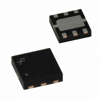
FPF2146 Fairchild Semiconductor, FPF2146 Datasheet - Page 10

FPF2146
Manufacturer Part Number
FPF2146
Description
IC LOAD SWITCH REV CURR BK 6-MLP
Manufacturer
Fairchild Semiconductor
Type
High Side Switchr
Datasheet
1.FPF2146.pdf
(13 pages)
Specifications of FPF2146
Number Of Outputs
1
Rds (on)
160 mOhm
Internal Switch(s)
Yes
Current Limit
400mA
Voltage - Input
1.8 ~ 5.5 V
Operating Temperature
-40°C ~ 85°C
Mounting Type
Surface Mount
Package / Case
6-MLP
Input Voltage
1.8 to 5.5V
Power Switch On Resistance
120mOhm
Output Current
400mA
Mounting
Surface Mount
Package Type
MLP EP
Operating Temperature (min)
-40C
Operating Temperature (max)
85C
Operating Temperature Classification
Industrial
Pin Count
6
Power Dissipation
1.2W
Lead Free Status / RoHS Status
Lead free / RoHS Compliant
Other names
FPF2146TR
FPF2140/42/43/44/46/47 Rev. D
Application Information
Typical Application
Input Capacitor
To limit the voltage drop on the input supply caused by transient
in-rush currents when the switch turns-on into a discharged load
capacitor or a short-circuit, a capacitor needs to be placed
between V
close to the pins is usually sufficient. Higher values of C
be used to further reduce the voltage drop.
Output Capacitor
A 0.1uF capacitor C
GND. This capacitor will prevent parasitic board inductances
from forcing V
FPF2140/42/44/46, the total output capacitance needs to be
kept below a maximum value, C
from registering an over-current condition and turning-off the
switch. The maximum output capacitance can be determined
from the following formula,
Power Dissipation
During normal operation as a switch, the power dissipation is
small and has little effect on the operating temperature of the
part. The parts with the higher current limits will dissipate the
most power and that will only be,
If the part goes into current limit the maximum power dissipation
will occur when the output is shorted to ground. For the
FPF2140/44,
Auto-Restart Time, t
t
BLANK
Battery
1.8V-5.5V
P(max) =
, so that the maximum power dissipated is,
P = (I
IN
C
=
OUT
and GND. A 0.1µF ceramic capacitor, C
OUT
LIM
the
t
30 + 450
BLANK
(max) =
below GND when the switch turns-off. For the
)
30
2
RSTRT
t
OUT
x R
BLANK
power
+ t
DS
, should be placed between V
RSTRT
C1 = 0.1µF
, and the Over Current Blanking Time,
x 5.5 x 0.8 = 275mW
= (0.8)
I
Typical value = 100KΩ
LIM
dissipation
(max) x t
OFF ON
OUT
x V
2
x 0.12 = 76.8mW
IN
(max), to prevent the part
V
(max) x I
IN
BLANK
will
(min)
LIM
scale
(max)
IN
OUT
, placed
by
V
ON
PGOOD
FPF2140/2/3/4/6/7
IN
IN
and
can
(1)
(3)
the
(2)
10
GND
When using the FPF2142/46 attention must be given to the
manual resetting of the part. The junction temperature will only
be allowed to increase to the thermal shutdown threshold. Once
this temperature has been reached, toggling ON will not turn-on
the switch until the junction temperature drops. For the
FPF2140/44, a short on the output will cause the part to operate
in a constant current state dissipating a worst case power as
calculated in (3) until the thermal shutdown activates. It will then
cycle in and out of thermal shutdown so long as the ON pin is
active and the short is present.
Board Layout
For best performance, all traces should be as short as possible.
To be most effective, the input and output capacitors should be
placed close to the device to minimize the effects that parasitic
trace inductances may have on normal and short-circuit
operation. Using wide traces for V
minimize parasitic electrical effects along with minimizing the
case to ambient thermal impedance.
The middle pad (pin 7) should be connected to the GND plate
of PCB for improving thermal performance of the load switch.
An improper layout could result higher junction temperature and
triggering the thermal shutdown protection feature. This concern
applies specially with FPF2143 and FPF2147 where load switch
turns on into an overcurrent condition and switch supplies
constant current limit value. In this case power dissipation of the
switch (P
maximum absolute power dissipation of 1.2W.
FLAGB
V
OUT
D
= (V
IN
- V
OUT
R1 = 100KΩ
C2 = 0.1µF
) x I
LIM
IN
(max)) could exceed the
, V
OUT
LOAD
and GND will help
www.fairchildsemi.com
R2 = 499Ω


