SI3861BDV-T1-E3 Vishay, SI3861BDV-T1-E3 Datasheet
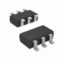
IC LOAD SWITCH LVL SHIFT 6-TSOP

SI3861BDV-T1-E3

Manufacturer Part Number
SI3861BDV-T1-E3
Description
IC LOAD SWITCH LVL SHIFT 6-TSOP
Manufacturer
Vishay
Type
High Side Switchr
Datasheet

Specifications of SI3861BDV-T1-E3

Number Of Outputs
1
Rds (on)
75 mOhm
Internal Switch(s)
Yes
Current Limit
2.3A
Voltage - Input
4.5 ~ 20 V
Operating Temperature
-55°C ~ 150°C
Mounting Type
Surface Mount
Package / Case
6-TSOP
On Resistance (max)
0.115 Ohm
Maximum Operating Temperature
+ 150 C
Minimum Operating Temperature
- 55 C
Maximum Power Dissipation
830 mW
Mounting Style
SMD/SMT
Switch Configuration
Dual
Transistor Polarity
N And P Channel
Continuous Drain Current Id
2.3A
Drain Source Voltage Vds
20V
On Resistance Rds(on)
145mohm
Rds(on) Test Voltage Vgs
10V
Power Dissipation Pd
830mW
Lead Free Status / RoHS Status
Lead free / RoHS Compliant
Lead Free Status / RoHS Status
Lead free / RoHS Compliant, Lead free / RoHS Compliant
Other names
SI3861BDV-T1-E3TR

Available stocks

Company
Part Number
Manufacturer
Quantity
Price
Part Number:
SI3861BDV-T1-E3
Manufacturer:
VISHAY
Quantity:
814
Document Number: 73343
S09-2110-Rev. B, 12-Oct-09
Note:
* Minimum R1 value should be at least 10 x R2 to ensure Q1 turn-on.
DESCRIPTION
The Si3861BDV includes a P- and N-Channel MOSFET in a
single TSOP-6 package. The low on-resistance P-Channel
TrenchFET
N-Channel, with an external resistor, can be used as a level-
APPLICATION CIRCUITS
ON/OFF
PRODUCT SUMMARY
COMPONENTS
R1
R2
C1
V
4.5 to 20
DS2
V
R2
IN
Optional Slew-Rate Control
(V)
C
R1
i
®
Pull-Up Resistor
is tailored for use as a load switch. The
4
6
5
0.120 at V
0.145 at V
0.075 at V
Si3861BDV
Q2
Q1
R
DS(on)
1
R2
IN
IN
IN
(Ω)
= 5.0 V
= 4.5 V
= 10 V
Load Switch with Level-Shift
2, 3
6
Typical 10 kΩ to 1 mΩ*
Typical 0 to 100 kΩ*
C
Typical 1000 pF
C1
o
I
± 1.9
± 1.7
D
± 2.3
(A)
V
GND
LOAD
OUT
FEATURES
The Si3861BDV is ideally suited for high-side load switching
in portable applications. The integrated N-Channel level-shift
device saves space by reducing external components. The
slew rate is set externally so that rise-times can be tailored to
different load types.
shift to drive the P-Channel load-switch. The N-Channel
MOSFET has internal ESD protection and can be driven by
logic signals as low as 1.5 V. The Si3861DV operates on
supply lines from 4.5 to 20 V, and can drive loads up to 2.3 A.
• Halogen-free According to IEC 61249-2-21
• 4.5 V Rated
• ESD Protected: 3000 V
• 105 mΩ Low R
• 4.5 V to 20 V Input
• 1.5 V to 8 V Logic Level Control
• Low Profile, Small Footprint TSOP-6 Package
• 3000 V ESD Protection On Input Switch, V
• Adjustable Slew-Rate
• Compliant to RoHS Directive 2002/95/EC
Definition
10
8
6
4
2
0
0
Note: For R2 switching variations with other V
DS(on)
2
combinations See Typical Characteristics
t
t
d(off)
d(on)
t
r
TrenchFET
4
R2 (kΩ)
6
Vishay Siliconix
®
t
f
Si3861BDV
8
I
V
C
C
L
ON/OFF
i
o
= 1 A
= 10 µF
= 1 µF
www.vishay.com
ON/OFF
10
= 3 V
IN
/R1
12
1

Related parts for SI3861BDV-T1-E3

SI3861BDV-T1-E3 Summary of contents

Page 1

... 0.120 5 0.145 4 DESCRIPTION The Si3861BDV includes a P- and N-Channel MOSFET in a single TSOP-6 package. The low on-resistance P-Channel ® TrenchFET is tailored for use as a load switch. The N-Channel, with an external resistor, can be used as a level- APPLICATION CIRCUITS Si3861BDV ...

Page 2

... Si3861BDV Vishay Siliconix FUNCTIONAL BLOCK DIAGRAM TSOP-6 Top View Ordering Information: Si3861BDV-T1-E3 (Lead (Pb)-free) Si3861BDV-T1-GE3 (Lead (Pb)-free and Halogen-free) ABSOLUTE MAXIMUM RATINGS T Parameter Input Voltage ON/OFF Voltage Load Current a Continuous Intrinsic Diode Conduction a Maximum Power Dissipation Operating Junction and Storage Temperature Range ESD Rating, MIL-STD-883D Human Body Model (100 pF, 1500 Ω ...

Page 3

... C J 0.3 0.2 0.1 0 2.0 1.8 1.6 1.4 1.2 1.0 0 °C J 0.6 0.4 0 2.0 1.8 1.6 1.4 1.2 1 0.8 0.6 0.4 0.2 0.0 100 125 150 Si3861BDV Vishay Siliconix ON/OFF T = 125 ° ° ( vs DROP 1 ON/OFF T = 125 ° ( ...

Page 4

... Si3861BDV Vishay Siliconix TYPICAL CHARACTERISTICS 25 °C, unless otherwise noted 1.8 1 1.4 1.2 1.0 0 ON/OFF 0.2 0.0 - 100 - Junction Temperature ( C) J Normalized On-Resistance vs. Junction Temperature d(off d(on (kΩ) Switching Variation kΩ IN 250 t d(off) 200 ON/OFF µF i 150 µF o 100 (kΩ) ...

Page 5

... ON/OFF µ µ d(on (kΩ) Switching Variation 4 300 kΩ Square Wave Pulse Dureation (s) Normalized Thermal Transient Impedance, Junction-to-Ambient Si3861BDV Vishay Siliconix t f 100 120 Notes Duty Cycle Per Unit Base = R = 150 C/W thJA ( thJA 4. Surface Mounted 1 0 100 www.vishay.com ...

Page 6

... Vishay product could result in personal injury or death. Customers using or selling Vishay products not expressly indicated for use in such applications their own risk and agree to fully indemnify and hold Vishay and its distributors harmless from and against any and all claims, liabilities, expenses and damages arising or resulting in connection with such use or sale, including attorneys fees, even if such claim alleges that Vishay or its distributor was negligent regarding the design or manufacture of the part ...

Related keywords