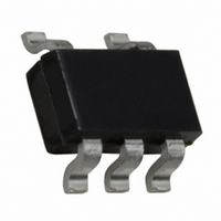
FPF2101 Fairchild Semiconductor, FPF2101 Datasheet - Page 10

FPF2101
Manufacturer Part Number
FPF2101
Description
IC SWITCH LOAD FULL FUNC SOT23-5
Manufacturer
Fairchild Semiconductor
Series
IntelliMax™r
Type
High Side Switchr
Datasheet
1.FPF2102.pdf
(12 pages)
Specifications of FPF2101
Number Of Outputs
1
Rds (on)
160 mOhm
Internal Switch(s)
Yes
Current Limit
200mA
Voltage - Input
1.8 ~ 5.5 V
Operating Temperature
-40°C ~ 85°C
Mounting Type
Surface Mount
Package / Case
SOT-23-5, SC-74A, SOT-25
Switch Type
Low Side
Power Switch Family
FPF2101
Input Voltage
1.8 to 5.5V
Power Switch On Resistance
160mOhm
Output Current
200mA
Mounting
Surface Mount
Package Type
SOT-23
Operating Temperature (min)
-40C
Operating Temperature (max)
85C
Operating Temperature Classification
Industrial
Pin Count
5
Power Dissipation
667mW
Package
5SOT-23
Lead Free Status / RoHS Status
Lead free / RoHS Compliant
Other names
FPF2101TR
FPF2101_NL
FPF2101_NLTR
FPF2101_NLTR
FPF2101_NL
FPF2101_NLTR
FPF2101_NLTR
Available stocks
Company
Part Number
Manufacturer
Quantity
Price
Company:
Part Number:
FPF2101
Manufacturer:
BROADCOM
Quantity:
8
Part Number:
FPF2101
Manufacturer:
FAIRCHILD/仙童
Quantity:
20 000
FPF2100-FPF2107 Rev. H
Application Information
Typical Application
Input Capacitor
To limit the voltage drop on the input supply caused by transient
in-rush currents when the switch turns-on into a discharged load
capacitor or a short-circuit, a capacitor needs to be placed
between V
placed close to the V
further reduce the voltage drop experienced as the switch is
turned on into a large capacitive load.
Output Capacitor
A 0.1uF capacitor C
GND. This capacitor will prevent parasitic board inductances
from forcing V
FPF2100-FPF2102 and the FPF2104-FPF2106, the total output
capacitance needs to be kept below a maximum value,
C
condition and turning off the switch. The maximum output
capacitance can be determined from the following formula,
Due to the integral body diode in the PMOS switch, a C
greater than C
C
removed. This could result in current flow through the body
diode from V
Power Dissipation
During normal operation as a switch, the power dissipation is
small and has little effect on the operating temperature of the
part. The parts with the higher current limits will dissipate the
most power and that will only typically be,
C
Battery
1.8V-5.5V
OUT
IN
P
OUT
can cause V
=
(max), to prevent the part from registering an over-current
(
(
max
I
LIM
IN
OUT
and GND. A 4.7µF ceramic capacitor, C
)
)
OUT
2
OUT
=
×
OUT
to V
R
below GND when the switch turns-off. For the
I
------------------------------------------------------------------- -
is highly recommended. A C
LIM
DS
OUT
IN
IN
to exceed V
(
pin. A higher value of C
.
max
=
, should be placed between V
C1 = 4.7µF
(
0.2
) t
×
V
)
OFF ON
2
IN
BLANK
IN
×
0.125
when the system supply is
(
min
=
)
IN
80mW
OUT
can be used to
greater than
IN
, must be
OUT
V
ON
FPF2100 - FPF2107
IN
(1)
(2)
and
IN
10
GND
If the part goes into current limit the maximum power dissipation
will occur when the output is shorted to ground. For the
FPF2100, FPF2101, FPF2104 and FPF2105, the power
dissipation will scale by the Auto-Restart Time, t
Over Current Blanking Time, t
power dissipated is typically,
When using the FPF2102 and FPF2106 attention must be given
to the manual resetting of the part. Continuously resetting the
part at a high duty cycle when a short on the output is present
can cause the temperature of the part to increase. The junction
temperature will only be allowed to increase to the thermal
shutdown threshold. Once this temperature has been reached,
toggling ON will not turn on the switch until the junction
temperature drops. For the FPF2103 and FPF2107, a short on
the output will cause the part to operate in a constant current
state dissipating a worst case power as calculated in (3) until
the thermal shutdown activates. It will then cycle in and out of
thermal shutdown so long as the ON pin is active and the short
is present.
Board Layout
For best performance, all traces should be as short as possible.
To be most effective, the input and output capacitors should be
placed close to the device to minimize the effects that parasitic
trace inductances may have on normal and short-circuit
operation. Using wide traces for V
minimize parasitic electrical effects along with minimizing the
case to ambient thermal impedance.
P max
(
FLAGB
V
OUT
)
=
=
---------------------- -
10
-------------------------------------------------- - xV
t
RESTART
10
+
160
t
BLANK
×
R1 = 100KΩ
+
C2 = 0.1µF
5.5
t
BLANK
×
BLANK
0.8
IN
, V
, so that the maximum
=
OUT
IN max
260mW
LOAD
(
and GND will help
)
www.fairchildsemi.com
xI
RSTRT
LIM max
R2 = 499Ω
, and the
(
)
(3)


