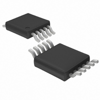
LTC4416IMS#TRPBF Linear Technology, LTC4416IMS#TRPBF Datasheet - Page 5

LTC4416IMS#TRPBF
Manufacturer Part Number
LTC4416IMS#TRPBF
Description
IC CNTRLR POWERPATH 10-MSOP
Manufacturer
Linear Technology
Series
PowerPath™r
Datasheet
1.LTC4416EMS-1PBF.pdf
(12 pages)
Specifications of LTC4416IMS#TRPBF
Applications
Battery Backup, Industrial/Automotive, High Current Switch
Fet Type
P-Channel
Number Of Outputs
2
Internal Switch(s)
No
Delay Time - On
60µs
Delay Time - Off
30µs
Voltage - Supply
3.6 V ~ 36 V
Current - Supply
130µA
Operating Temperature
-40°C ~ 125°C
Mounting Type
Surface Mount
Package / Case
10-MSOP, Micro10™, 10-uMAX, 10-uSOP
Lead Free Status / RoHS Status
Lead free / RoHS Compliant
Available stocks
Company
Part Number
Manufacturer
Quantity
Price
PI FU CTIO S
H1 (Pin 1): Open-Drain Comparator Output of the E1 Pin.
If E1 > V
the pin will be grounded. The maximum voltage permitted
on this pin is 7V. This pin provides support for setting up
hysterisis to an external resistor network.
E1 (Pin 2): LTC4416 Comparator Enable Input. A high
signal greater than V
diode action will then determine if the V1 path should turn
on by controlling any PFET(s) connected to the G1 pin.
If the E1 signal is driven low, the V1 path will perform a
“soft-off” provided the PFET(s) are properly configured
for blocking DC current. An internal current sink will pull
the E1 pin down when the E1 input exceeds 1.5V.
E1 (Pin 2): LTC4416-1 Comparator Enable Input. A high
signal greater than V
diode action will then determine if the V1 path should turn
on by controlling any PFET(s) connected to the G1 pin.
If the E1 signal is driven low, the V1 path will be quickly
disabled by enabling the “fast-off” feature, pulling the G1
gate high. An internal current sink will pull the E1 pin down
when the E1 input exceeds 1.5V.
GND (Pin 3): Ground. This pin provides a power return
path for all the internal circuits.
E2 (Pin 4): LTC4416 Comparator Enable Input. A low
signal less than V
diode action will then determine if the V2 path should turn
on by controlling any PFET(s) connected to the G2 pin.
If the E2 signal is driven high, the V2 path will perform a
“soft-off” provided the PFET(s) are properly configured
for blocking DC current. An internal current sink will pull
the E2 pin down when the E2 input exceeds 1.5V.
E2 (Pin 4): LTC4416-1 Comparator Enable Input. A low
signal less than V
diode action will then determine if the V2 path should turn
on by controlling any PFET(s) connected to the G2 pin.
If the E2 signal is driven high, the V2 path will be quickly
disabled by enabling the “fast-off” feature, pulling the G2
gate high. An internal current sink will pull the E2 pin down
when the E2 input exceeds 1.5V.
H2 (Pin 5): Open-Drain Comparator Output of the E2 Pin.
If E2 > V
U
REF
REF
U
, the H1 pin will go high impedance, otherwise
, the H2 pin will go high impedance, otherwise
REF
REF
REF
REF
U
will enable the V2 path. The ideal
will enable the V2 path. The ideal
will enable the V1 path. The ideal
will enable the V1 path. The ideal
the pin will be grounded. The maximum voltage permitted
on this pin is 7V. This pin provides support for setting up
hysterisis to an external resistor network.
G2 (Pin 6): Second P-Channel MOSFET Power Switch
Gate Drive Pin. This pin is directed by the second power
controller to maintain a forward regulation voltage (V
of 25mV between the V2 and V
than V
to the V
power switch.
V2 (Pin 7): Second Input Supply Voltage. Supplies power
to the second power controller and the band-gap refer-
ence. V2 is one of the two voltage sense inputs to the
second internal power controller (the other input to the
second internal power controller is the V
is usually supplied power from the second, or backup,
power source. This pin can be bypassed to ground with
a capacitor in the range of 0.1µF to 10µF if needed to
suppress load transients.
V
the internal circuitry of both the first and second power
controller and the band-gap reference. This pin is also a
voltage sense input to both internal analog controllers
(the other input to the first controller is the V1 pin and
the other input to the second controller is the V2 pin.)
This input may also be supplied power from an auxiliary
source which also supplies current to the load.
V1 (Pin 9): First Input Supply Voltage. Supplies power to
the first power controller and the band-gap reference. V1
is one of the two voltage sense inputs to the first internal
power controller (the other input to the first internal power
controller is the V
power from the first, or primary, power source. This pin
can be bypassed to ground with a capacitor in the range
of 0.1µF to 10µF if needed to suppress load transients.
G1 (Pin 10): First P-Channel MOSFET Power Switch Gate
Drive Pin. This pin is directed by the first power controller
to maintain a forward regulation voltage (V
between the V1 and V
When V1 is less than V
voltage, turning off the first P-channel power switch.
S
(Pin 8): Power Sense Input Pin. Supplies power to
S
. When V2 is less than V
S
pin voltage, turning off the second P-channel
LTC4416/LTC4416-1
S
pin). This input is usually supplied
S
S
, the G1 pin will pull up to the V
pins when V1 is greater than V
S
S
pins when V2 is greater
, the G2 pin will pull up
S
pin). This input
FR
) of 25mV
S
4416fa
pin
FR
S
)
.


