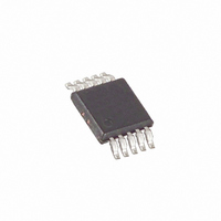
MAX8555AEUB+ Maxim Integrated Products, MAX8555AEUB+ Datasheet - Page 2

MAX8555AEUB+
Manufacturer Part Number
MAX8555AEUB+
Description
IC CNTRLR MOSFET ORING 10-UMAX
Manufacturer
Maxim Integrated Products
Datasheet
1.MAX8555AEUB.pdf
(17 pages)
Specifications of MAX8555AEUB+
Applications
Telecom Supplies, Rectifiers
Fet Type
N-Channel
Number Of Outputs
1
Internal Switch(s)
No
Delay Time - Off
100ns
Voltage - Supply
8 V ~ 13.25 V
Current - Supply
2mA
Operating Temperature
-40°C ~ 85°C
Mounting Type
Surface Mount
Package / Case
10-MSOP, Micro10™, 10-uMAX, 10-uSOP
Lead Free Status / RoHS Status
Lead free / RoHS Compliant
Delay Time - On
-
Lead Free Status / Rohs Status
Lead free / RoHS Compliant
ABSOLUTE MAXIMUM RATINGS
GATE to GND .........................................................-0.3V to +12V
FAULT, VL to GND ...................................................-0.3V to +6V
OVP, UVP, TIMER, CS+, CS- to GND .......-0.3V to +(V
V
Continuous Power Dissipation (T
Low-Cost, High-Reliability, 0.5V to 3.3V ORing
MOSFET Controllers
Stresses beyond those listed under “Absolute Maximum Ratings” may cause permanent damage to the device. These are stress ratings only, and functional
operation of the device at these or any other conditions beyond those indicated in the operational sections of the specifications is not implied. Exposure to
absolute maximum rating conditions for extended periods may affect device reliability.
ELECTRICAL CHARACTERISTICS
(V
T
2
DD
V
V
V
V
V
Threshold
VL SUPPLY
VL Input Voltage
VL Supply Current
VL Current in Shutdown Mode
VL Output Voltage
VL Undervoltage Lockout
CS INPUTS
CS+, CS- Input Current
Offset Input Current (CS+, CS-)
CS+/CS- Input Range
CS Isolation
CHARGE-PUMP VOLTAGE
GATE Voltage, V
Charge-Pump Switching
Frequency
A
DD
10-Pin µMAX (derate 5.6mW/°C above +70°C) ...........444mW
10-Pin TDFN (derate 24.4mW/°C above +70°C) .......1951mW
DD
DD
DD
DD
DD
= 0°C to +85°C, unless otherwise noted.)
_______________________________________________________________________________________
to GND..................................................(V
= 12V, V
SUPPLY
Input Voltage
Supply Current
Shutdown Current
Overvoltage Internal
PARAMETER
CS-
GATE
= 1.4V, V
CS+
= 1.5V, R
A
= +70°C)
V
VL unconnected, V
V
V
Rising threshold
Falling threshold
V
V
TIMER = GND, V
V
VL = V
VL = V
V
V
(Note 1)
V
V
Measured from GATE to CS+
R
R
R
V
TIMER
DD
TIMER
DD
DD
DD
TIMER
CS
CS+
CS-
TIMER
TIMER
TIMER
TIMER
= 3.0V, Figure 4
TIMER
= V
= V
= V
= 8V to 13.25V, I
= +3V, V
= +3V, V
DD
DD
= 2.5V
= 0V, V
= 2.5V, V
= 20k
= 125k
= open
= 1.5V
VL
VL
VL
VL
, rising threshold
, falling threshold
= 5V, V
= 5V, V
= 25kΩ, V
- 0.3V) to +18V
CS+
CS-
DD
VL
DD
CS
TIMER
TIMER
= 13.25V
= 0V, I
= 0V, I
+ 0.3V)
TIMER
= 3.0V
= V
UVP
VL
VL unconnected
VL = V
CONDITIONS
VL
= 0A
= 2.5V
= 2.5V
CS-
CS+
= 2.5V, V
= 1V, V
= 5V
DD
V
V
Operating Temperature Range ...........................-40°C to +85°C
Junction Temperature ......................................................+150°C
Storage Temperature Range .............................-65°C to +150°C
Lead Temperature (soldering, 10s) .................................+300°C
DD
DD
OVP
DD
= 8V to 13.25V
= V
= 13.25V
= 0.25V, R
VL
= 5V
FAULT
= 50kΩ, C
-250
MIN
8.00
14.0
13.3
3.80
2.78
2.68
3.0
3.0
0.5
5.0
VDD
TYP
0.04
14.4
13.8
2.82
2.75
5.25
= C
-0.5
-0.5
187
450
500
550
2.0
1.8
1.6
4.1
5.2
GATE
V
13.25
VL
MAX
+250
= C
15.0
14.5
4.45
2.90
2.82
5.5
3.3
0.2
3.0
5.5
3.0
3.0
5.5
- 0.5
VL
= 0.01µF,
UNITS
kHz
mA
mA
mA
mA
µA
nA
µA
V
V
V
V
V
V
V


