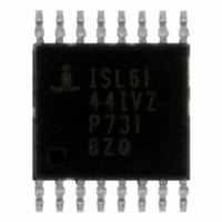
ISL6144IVZA Intersil, ISL6144IVZA Datasheet - Page 6

ISL6144IVZA
Manufacturer Part Number
ISL6144IVZA
Description
IC CTRLR MOSFET ORING HV 16TSSOP
Manufacturer
Intersil
Datasheet
1.ISL6144IVZA.pdf
(29 pages)
Specifications of ISL6144IVZA
Applications
Telecom/Datacom Systems
Fet Type
N-Channel
Number Of Outputs
1
Internal Switch(s)
No
Delay Time - On
1ms
Delay Time - Off
250ns
Voltage - Supply
10 V ~ 75 V
Operating Temperature
-40°C ~ 105°C
Mounting Type
Surface Mount
Package / Case
16-TSSOP
Lead Free Status / RoHS Status
Lead free / RoHS Compliant
Current - Supply
-
Available stocks
Company
Part Number
Manufacturer
Quantity
Price
Company:
Part Number:
ISL6144IVZA
Manufacturer:
Intersil
Quantity:
304
Part Number:
ISL6144IVZA
Manufacturer:
INTERSIL
Quantity:
20 000
Company:
Part Number:
ISL6144IVZA-T
Manufacturer:
ST
Quantity:
3 200
Electrical Specifications
NOTES:
Functional Pin Description
GATE
This is the Gate Drive output of the external N-Channel
MOSFET generated by the IC internal charge pump. Gate
turn-on time is typically 1ms.
VIN
Input bias pin connected to the sourcing supply side (ORing
MOSFET Source). Also serves as the sense pin to
determine the sourcing supply voltage. The ORing MOSFET
will be turned off when VIN becomes lower than VOUT by a
value more than the externally set threshold.
VOUT
Connected to the Load side (ORing MOSFET Drain). This is
the VOUT sense pin connected to the load. This is the
common connection point for multiple paralleled supplies.
VOUT is compared to VIN to determine when the ORing
FET has to be turned off.
HVREF
Low side of the internal IC High Voltage Reference used by
internal circuitry, also available as an external pin for
additional external capacitor connection.
COMP
This is the high side connection for the HS Comparator trip
level setting (V
COMP and V
V
externally set the desired level depending on particular
system requirement.
VSET
Low side connection for the HS Comparator trip level setting
A second resistor R
provides adjustable “V
VSET Voltage (V
Fault Low Output Voltage
Fault Sink Current
Fault Leakage Current
Fault Delay - Low to High
9. Compliance to datasheet limits is assured by one or more methods: production test, characterization and/or design.
OUT
- V
PARAMETER
IN
trip level (0V to 5V). This provides flexibility to
OUT
TH(HS)
OUT
along with resistor R
- VSET)
2
connected between VSET and COMP
). Resistor R
IN
- V
OUT
6
V
temperature range, -40°C to +105°C.
V
” level along with R
I
IN
I
SYMBOL
REF(VSET)
FLT_LEAK
FLT_SINK
V
1
= 48V, T
T
FLT_L
, connected between
FLT
2
, provides adjustable
A
= -40°C to +105°C, Unless Otherwise Specified. Boldface limits apply over the operating
V
V
FAULT = V
FAULT = ”V
GATE = V
IN
IN
= 9V to 75V
- V
OUT
1
.
GL
FLT_L
FLT_H
< 0V, V
to FAULT
TEST CONDITIONS
ISL6144
, V
”, V
GATE
IN
IN
< V
=
> V
V
= V
OUT
OUT
FLT_L
FAULT
Open-Drain pull-down FAULT Output with internal on-chip
filtering (
pull-down this pin to GND as soon as it detects a fault.
Different types of faults and their detection mechanisms are
discussed in more detail in the “Functional Block Description”
on page 6.
GND
IC ground reference.
Detailed Description
The ISL6144 and a suitably sized N-Channel power
MOSFET(s) increases power distribution efficiency and
availability when replacing a power ORing diode in high current
applications. Refer to “Application Considerations” on page 8
for power saving when using ISL6144 with an N-channel ORing
MOSFET compared to a typical ORing diode.
Functional Block Description
Regulating Amplifier-Slow (Quiet) Turn-off
A Hysteretic Regulating (HR) Amplifier is used for a
Quiet/Slow turn-off mechanism. This slow turn-off is initiated
when the sourcing power supply is turned off slowly for
system diagnostics. Under normal operating conditions as
V
HR Amplifier regulates the gate voltage to keep the 20mV
(
(Vs - Vd). This will continue until the load current exceeds
the MOSFET ability to deliver the current with Vsd of 20mV.
In this case, Gate will be charged to the full charge pump
voltage (V
the MOSFET will be fully enhanced and behave as a
constant resistor valued at the r
drop below V
output of the HR Amp is pulled high and the gate is pulled
down to V
ORing FET is turned off, avoiding reverse current as well as
voltage and current stresses on supply components.
GL
V
, V
OUT
FWD_HR
, V
GATE
GATE
pulls up to 20mV below V
T
= V
FLT
= V
) forward voltage drop across the ORing MOSFET
GQP
IN
GL
IN
). The ISL6144 fault detection circuitry will
slowly in less than a 100µs. As a result, the
OUT
) to fully enhance the MOSFET. At this point,
+ V
, regulation cannot be maintained and the
GQP
(Note 9)
MIN
4
-
-
-
-
DS(ON)
IN
(V
TYP
120
5.3
IN
-
-
-
. Once V
- 20mV > V
(Note 9) UNITS
MAX
0.5
10
IN
-
-
-
January 6, 2011
starts to
OUT
FN9131.6
), the
mA
µA
µs
V
V


