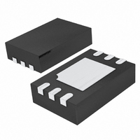
LTC4357HDCB#TRMPBF Linear Technology, LTC4357HDCB#TRMPBF Datasheet - Page 7

LTC4357HDCB#TRMPBF
Manufacturer Part Number
LTC4357HDCB#TRMPBF
Description
IC CTRLR IDEAL DIODE 6-DFN
Manufacturer
Linear Technology
Datasheet
1.LTC4357CDCBTRMPBF.pdf
(14 pages)
Specifications of LTC4357HDCB#TRMPBF
Applications
Redundant Power Supplies, Telecom Infrastructure
Fet Type
N-Channel
Number Of Outputs
1
Internal Switch(s)
No
Delay Time - Off
300ns
Voltage - Supply
9 V ~ 80 V
Current - Supply
500µA
Operating Temperature
-40°C ~ 125°C
Mounting Type
Surface Mount
Package / Case
6-DFN
Operating Temperature (max)
125C
Operating Temperature (min)
-40C
Pin Count
6
Mounting
Surface Mount
Package Type
DFN EP
Case Length
2mm
Screening Level
Automotive
Lead Free Status / RoHS Status
Lead free / RoHS Compliant
Delay Time - On
-
Lead Free Status / Rohs Status
Compliant
Other names
LTC4357HDCB#TRMPBF
Available stocks
Company
Part Number
Manufacturer
Quantity
Price
applications inForMation
Load Sharing
The application in Figure 1 combines the outputs of multiple,
redundant supplies using a simple technique known as
droop sharing. Load current is first taken from the highest
output, with the low outputs contributing as the output
voltage falls under increased loading. The 25mV regulation
technique ensures smooth load sharing between outputs
without oscillation. The degree of sharing is a function of
R
initial output voltages.
DS(ON)
PSA
PSB
PSC
RTNA
RTNB
RTNC
V
V
V
48V
48V
48V
, the output impedance of the supplies and their
INA
INB
INC
Figure 1. Droop Sharing Redundant Supplies
IN
IN
IN
FDB3632
LTC4357
FDB3632
LTC4357
FDB3632
LTC4357
GATE
GATE
GATE
GND
GND
GND
M1
M2
M3
OUT
OUT
OUT
V
V
V
4357 F01
DD
DD
DD
48V BUS
Input Short-Circuit Faults
The dynamic behavior of an active, ideal diode entering
reverse bias is most accurately characterized by a delay
followed by a period of reverse recovery. During the delay
phase some reverse current is built up, limited by parasitic
resistances and inductances. During the reverse recovery
phase, energy stored in the parasitic inductances is trans-
ferred to other elements in the circuit. Current slew rates
during reverse recovery may reach 100A/µs or higher.
High slew rates coupled with parasitic inductances in se-
ries with the input and output paths may cause potentially
destructive transients to appear at the IN and OUT pins
of the LTC4357 during reverse recovery. A zero imped-
ance short-circuit directly across the input of the circuit
is especially troublesome because it permits the highest
possible reverse current to build up during the delay phase.
When the MOSFET finally commutates the reverse current
the LTC4357 IN pin experiences a negative voltage spike,
while the OUT pin spikes in the positive direction.
To prevent damage to the LTC4357 under conditions of
input short-circuit, protect the IN pin and OUT pin as
shown in Figure 2. The IN pin is protected by clamping
to the GND pin in the negative direction. Protect the OUT
pin with a clamp, such as with a TVS or TransZorb, or with
a local bypass capacitor of at least 10µF . In low voltage
applications the MOSFET's drain-source breakdown may
be sufficient to protect the OUT pin, provided BV
V
Parasitic inductance between the load bypass and the
LTC4357 allows a zero impedance input short to collapse
the voltage at the V
time (t
with 39µF; above 30V use at least 100µF . If V
from the output side, one capacitor serves to guard against
V
If the OUT pin is protected by a diode clamp or if V
powered from the input side, decouple the V
separate 100Ω, 100nF filter (see Figure 3). In applications
above 10A increase the filter capacitor to 1µF .
IN
DD
< 100V.
collapse and also protect OUT from voltage spikes.
OFF
). For applications up to 30V, bypass the V
DD
pin, which increases the total turn-off
LTC4357
DD
DD
is powered
pin with a
DD
DSS
DD
4357fd
pin
is
+


