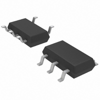
LTC4411ES5#TRMPBF Linear Technology, LTC4411ES5#TRMPBF Datasheet - Page 4

LTC4411ES5#TRMPBF
Manufacturer Part Number
LTC4411ES5#TRMPBF
Description
IC IDEAL DIODE LOW LOSS TSOT23-5
Manufacturer
Linear Technology
Datasheet
1.LTC4411ES5TRMPBF.pdf
(8 pages)
Specifications of LTC4411ES5#TRMPBF
Applications
Handheld/Mobile Devices
Fet Type
P-Channel
Number Of Outputs
1
Internal Switch(s)
Yes
Delay Time - On
1.2µs
Delay Time - Off
1.1µs
Voltage - Supply
2.6 V ~ 5.5 V
Current - Supply
40µA
Operating Temperature
-40°C ~ 85°C
Mounting Type
Surface Mount
Package / Case
TSOT-23-5, TSOT-5, TSOP-5
Lead Free Status / RoHS Status
Lead free / RoHS Compliant
Other names
LTC4411ES5#PBF
LTC4411ES5#PBF
LTC4411ES5#TRMPBF
LTC4411ES5#TRMPBFTR
LTC4411ES5#PBF
LTC4411ES5#TRMPBF
LTC4411ES5#TRMPBFTR
Available stocks
Company
Part Number
Manufacturer
Quantity
Price
LTC4411
TYPICAL PERFOR A CE CHARACTERISTICS
PI FU CTIO S
4
IN (Pin 1): Ideal Diode Anode and Positive Power Supply
for LTC4411. When operating LTC4411 as a switch it must
be bypassed with a low ESR ceramic capacitor of 1µF. X5R
and X7R dielectrics are preferred for their superior voltage
and temperature characteristics.
GND (Pin 2): Power and Signal Ground for the IC.
CTL (Pin 3): Controlled Shutdown Pin. Weak (3µA) Pull-
Down. Pull this pin high to shut down the IC. Tie to GND
to enable. Can be left floating when not in use.
0.150
0.125
0.100
0.075
0.050
100n
U
10µ
10n
1µ
2.5
0
R
I
LEAK
FWD
U
3.0
1
vs V
vs V
T
T
T
T
T
T
T
A
A
A
A
A
A
A
= –40°C
= 0°C
= 40°C
= 60°C
= 80°C
= 100°C
= 120°C
REVERSE VOLTAGE (V)
SUPPLY VOLTAGE (V)
REVERSE
SUPPLY
3.5
2
U
4.0
3
, V
IN
T
T
4.5
4
A
A
= 0V
= 80°C
= 120°C
W
5.0
5
U
4411 G04
4411 G07
5.5
6
500mV/DIV
500mA/DIV
2V/DIV
2V/DIV
V
V
V
CTRL
STAT
I
0.20
0.15
0.10
0.05
OUT
OUT
0
–40
R
V
CTL Turn-On
FWD
IN
–20
= 3.6V
vs Temperature at
0
TEMPERATURE (°C)
20
200µs/DIV
STAT (Pin 4): Status Condition Indicator. This pin indi-
cates the conducting status of the LTC4411. If the part is
forward biased (V
If the part is reverse biased (V
pin will pull down 10µA through an open-drain. When
terminated to a high voltage through a 470k resistor, a
high voltage indicates diode conducting. May be left
floating or grounded when not in use.
OUT (Pin 5): Ideal Diode Cathode and Output of the
LTC4411. Bypass OUT with a nominal 1mΩ ESR capacitor
of at least 4.7µF. The LTC4411 is stable with ESRs down
to 0.2mΩ. However stability improves with higher ESRs.
40
60
80
100
4411 G05
4411 G08
120
500mV/DIV
IN
50mA/DIV
> V
2V/DIV
2V/DIV
V
V
100µ
100n
CTRL
STAT
V
I
10µ
OUT
OUT
1µ
OUT
0
I
CTL Turn-Off
QROUT
+ V
OUT
1
FWD
vs V
REVERSE VOLTAGE (V)
> V
) this pin will be Hi-Z.
REVERSE
2
IN
20µs/DIV
+ V
3
RTO
at V
4
IN
), then this
T
T
T
T
T
= 0V
A
A
A
A
A
= –40°C
= 0°C
= 40°C
= 80°C
= 120°C
5
4411 G06
4411 G09
4411fa
6


