LMD18245T/NOPB National Semiconductor, LMD18245T/NOPB Datasheet - Page 3
LMD18245T/NOPB
Manufacturer Part Number
LMD18245T/NOPB
Description
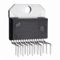
IC H BRIDGE 3A 55V TO-220
Manufacturer
National Semiconductor
Datasheet
1.LMD18245TNOPB.pdf
(21 pages)
Specifications of LMD18245T/NOPB
Applications
DC Motor Driver, Stepper Motor Driver, H Bridge
Number Of Outputs
1
Current - Output
3A
Voltage - Supply
12 V ~ 55 V
Operating Temperature
-40°C ~ 125°C
Mounting Type
Through Hole
Package / Case
TO-220-15 (Bent and Staggered Leads)
Operating Temperature Classification
Automotive
Package Type
TO-220
Operating Supply Voltage (min)
12V
Operating Supply Voltage (max)
55V
Lead Free Status / RoHS Status
Lead free / RoHS Compliant
Voltage - Load
-
Lead Free Status / Rohs Status
Compliant
Other names
*LMD18245T
*LMD18245T/NOPB
LMD18245T
*LMD18245T/NOPB
LMD18245T
Available stocks
Company
Part Number
Manufacturer
Quantity
Price
Company:

Part Number:
LMD18245T/NOPB
Manufacturer:
ST
Quantity:
14 300
Part Number:
LMD18245T/NOPB
Manufacturer:
NS/国半
Quantity:
20 000


I
POWER OUTPUT STAGE
R
V
T
Q
t
t
t
t
t
t
CURRENT SENSE AMPLIFIER
CC
D(ON)
D(OFF)
ON
OFF
pw
DB
Symbol
rr
DIODE
DS(ON)
Absolute Maximum Ratings
If Military/Aerospace specified devices are required,
please contact the National Semiconductor Sales Office/
Distributors for availability and specifications.
Electrical Characteristics
The following specifications apply for V
perature range, −40˚C
rr
DC Voltage at:
DC Voltage PGND to SGND
Continuous Load Current
Peak Load Current (Note 2)
Junction Temperature (T
Power Dissipation (Note 3) :
OUT 1, V
COMP OUT, RC, M4, M3, M2, M1, BRAKE,
DIRECTION, CS OUT, and DAC REF
Quiescent Supply Current
Switch ON Resistance
Body Diode Forward Voltage
Diode Reverse Recovery Time
Diode Reverse Recovery Charge
Output Turn ON Delay Time
Output Turn OFF Delay Time
Output Turn ON Switching Time
Output Turn OFF Switching Time
Minimum Input Pulse Width
Minimum Dead Band
Current Sense Output
Current Sense Linearity Error
CC
Sourcing Outputs
Sinking Outputs
Sourcing Outputs
Sinking Outputs
Sourcing Outputs
Sinking Outputs
Sourcing Outputs
Sinking Outputs
, and OUT 2
Parameter
J(max)
T
J
)
+125˚C. All other limits apply for T
CC
= +42V, unless otherwise stated. Boldface limits apply over the operating tem-
(Note 2)
(Note 1)
DAC REF = 0V, V
I
I
I
I
I
I
I
I
I
I
I
I
I
Pins 10 and 11
(Note 6)
I
0.5A
LOAD
LOAD
DIODE
DIODE
DIODE
LOAD
LOAD
LOAD
LOAD
LOAD
LOAD
LOAD
LOAD
LOAD
±
+150˚C
400mV
+60V
+12V
= 3A
= 6A
= 3A
= 3A
= 3A
= 3A
= 3A
= 3A
= 3A
= 3A
= 1A (Note 7)
= 3A
= 1A
= 1A
I
3A
6A
LOAD
Conditions
3
3A (Note 7)
A
CC
Operating Conditions
= T
ESD Susceptibility (Note 4)
Storage Temperature Range (T
Lead Temperature (Soldering, 10 seconds)
Temperature Range (T
Supply Voltage Range (V
CS OUT Voltage Range
DAC REF Voltage Range
MONOSTABLE Pulse Range
= +20V
TO-220 (T
TO-220 (T
J
= 25˚C.
A
A
= 25˚C, Infinite Heatsink)
= 25˚C, Free Air)
(Note 5)
Typical
J
900
600
400
200
250
0.3
0.3
1.0
±
80
40
40
80
40
) (Note 3)
8
5
1
2
6
CC
)
S
)
(Note 5)
(Note 1)
Limit
200
175
300
325
0.4
0.6
0.4
0.6
1.5
15
±
9
−40˚C to +150˚C
−40˚C to +125˚C
10 µs to 100 ms
+12V to +55V
www.national.com
0V to +5V
0V to +5V
mA (max)
µA (max)
µA (max)
µA (min)
µA (min)
(Limits)
%(max)
V(max)
1500V
Units
300˚C
mA
(max)
(max)
(max)
(max)
3.5W
nC
ns
µs
ns
ns
ns
µs
µs
ns
ns
µs
ns
25W
%
V
Related parts for LMD18245T/NOPB
Image
Part Number
Description
Manufacturer
Datasheet
Request
R

Part Number:
Description:
IC MOTOR DRIVER FULL BRIDGE 3A TO-220-15
Manufacturer:
National Semiconductor
Datasheet:

Part Number:
Description:
H-BRIDGE MOTOR DRIVER W/ PWM
Manufacturer:
National Semiconductor
Part Number:
Description:
Manufacturer:
National Semiconductor
Datasheet:

Part Number:
Description:
3a, 55v Dmos Full-bridge Motor Driver
Manufacturer:
National Semiconductor Corporation
Datasheet:
Part Number:
Description:
National Semiconductor [8-Bit D/A Converter]
Manufacturer:
National Semiconductor
Datasheet:
Part Number:
Description:
National Semiconductor [Media Coprocessor]
Manufacturer:
National Semiconductor
Datasheet:
Part Number:
Description:
Digitally Controlled Tone and Volume Circuit with Stereo Audio Power Amplifier, Microphone Preamp Stage and National 3D Sound
Manufacturer:
National Semiconductor
Datasheet:
Part Number:
Description:
Digitally Controlled Tone and Volume Circuit with Stereo Audio Power Amplifier, Microphone Preamp Stage and National 3D Sound
Manufacturer:
National Semiconductor
Datasheet:
Part Number:
Description:
AC97 Rev 2 Codec with Sample Rate Conversion and National 3D Sound
Manufacturer:
National Semiconductor
Part Number:
Description:
Manufacturer:
National Semiconductor
Datasheet:
Part Number:
Description:
Manufacturer:
National Semiconductor
Datasheet:
Part Number:
Description:
General Purpose, Low Voltage, Low Power, Rail-to-Rail Output Operational Amplifiers
Manufacturer:
National Semiconductor
Datasheet:
Part Number:
Description:
8-bit 20 MSPS flash A/D converter.
Manufacturer:
National Semiconductor
Datasheet:
Part Number:
Description:
Low Noise Quad Operational Amplifier
Manufacturer:
National Semiconductor
Datasheet: