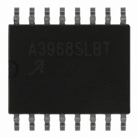
A3968SLBTR-T Allegro Microsystems Inc, A3968SLBTR-T Datasheet - Page 7

A3968SLBTR-T
Manufacturer Part Number
A3968SLBTR-T
Description
IC MOTOR DRIVER PWM DUAL 16SOIC
Manufacturer
Allegro Microsystems Inc
Datasheet
1.A3968SLBTR-T.pdf
(8 pages)
Specifications of A3968SLBTR-T
Applications
PWM Motor Driver
Number Of Outputs
2
Current - Output
±650mA
Voltage - Load
4.75 V ~ 30 V
Voltage - Supply
4.75 V ~ 5.5 V
Operating Temperature
-20°C ~ 85°C
Mounting Type
Surface Mount
Package / Case
16-SOIC (0.300", 7.5mm Width)
Motor Type
Full Bridge
No. Of Outputs
2
Output Current
650mA
Output Voltage
30V
Supply Voltage Range
4.75V To 5.5V
Driver Case Style
SOIC
No. Of Pins
16
Lead Free Status / RoHS Status
Lead free / RoHS Compliant
Other names
620-1141-2
A3968SLBTR-T
A3968SLBTR-T
Available stocks
Company
Part Number
Manufacturer
Quantity
Price
Part Number:
A3968SLBTR-T
Manufacturer:
ALLEGRO/雅丽高
Quantity:
20 000
A3968
Load Current Regulation. Due to internal logic and
switching delays, t
slightly higher than the I
blanking time, limit the minimum value the current control
circuitry can regulate. To produce zero current in a wind-
ing, the INPUT
high, turning off all output drivers for that full-bridge.
Logic Inputs. The direction of current in the motor wind-
ing is determined by the state of the INPUT
terminals of each bridge (see Truth Table). An internally
generated dead time, t
cross-over current spikes that can occur when switching the
motor direction.
A logic high on both INPUTs turns off all four output driv-
ers of that full-bridge. This results in a fast current decay
through the internal ground clamp and fl yback diodes.
The appropriate INPUT
modulated for applications that require a fast current-de-
cay PWM. If external current-sensing circuitry is used, the
internal current-control logic can be disabled by connecting
the R
A logic low on the INPUT
place that full-bridge in the brake mode. Both source driv-
ers are turned off and both sink drivers are turned on. This
has the effect of shorting the DC motor back-EMF voltage,
resulting in a current fl ow that dynamically brakes the mo-
tor. Note that, during braking, the internal current-control
circuitry is disabled. Therefore, care should be taken to
ensure that the motor current does not exceed the absolute
maximum rating of the A3968.
resistor divider from V
nally divided down by 4 to set up the current-comparator
trip-voltage threshold. The reference input voltage range is
0 to 2 V.
The REFERENCE input voltage is typically set with a
T
C
T
terminal to ground.
A
and INPUT
d
, the actual load current peak will be
codt
CC
A
TRIP
. This reference voltage is inter-
, of approximately 1.8 μs prevents
or INPUT
A
and the INPUT
B
value. These delays, plus the
Dual Full-Bridge PWM Motor Driver with Brake
terminals should be held
FUNCTIONAL DESCRIPTION (continued)
B
can be pulse-width
B
A
terminals will
and INPUT
B
Output Drivers. To minimize on-chip power dissipa-
tion, the sink drivers incorporate a Satlington structure.
The Satlington output combines the low V
of a saturated transistor and the high peak-current capabil-
ity of a Darlington (connected) transistor. A graph showing
typical output saturation voltages as a function of output
current is on page 5.
Miscellaneous Information. Thermal protection
circuitry turns off all output drivers should the junction
temperature reach 165 °C typical. This is intended only to
protect the device from failures due to excessive junction
temperatures and should not imply that output short circuits
are permitted. Normal operation is resumed when the junc-
tion temperature has decreased about 15°C.
variable duty cycle PWM technique. As a result, the cur-
rent-control regulation may become unstable if the duty
cycle exceeds 50%.
ground trace I
have a separate return to the ground terminal of the device.
For low-value sense resistors, the I x R drops in the printed-
wiring board can be signifi cant and should be taken into ac-
count. The use of sockets should be avoided as their contact
resistance can cause variations in the effective value of R
pled with an electrolytic capacitor (47 μF recommended)
placed as close to the device as physically practical. To
minimize the effect of system ground I x R drops on the
logic and reference input signals, the system ground should
have a low-resistance return to the load supply voltage.
amount of ripple current. A lower frequency will result in
higher current ripple, but reduced heating in the motor and
driver IC due to a corresponding decrease in hysteretic core
losses and switching losses respectively. A higher frequen-
cy will reduce ripple current, but will increase switching
losses and EMI.
The A3968 current control employs a fi xed-frequency,
To minimize current-sensing inaccuracies caused by
The LOAD SUPPLY terminal, V
The frequency of the clock oscillator will determine the
R
drops, each current-sensing resistor should
115 Northeast Cutoff, Box 15036
Allegro MicroSystems, Inc.
Worcester, Massachusetts 01615-0036 (508) 853-5000
www.allegromicro.com
BB
, should be decou-
CE(sat)
features
S
.
7


