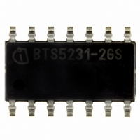
BTS5231-2GS Infineon Technologies, BTS5231-2GS Datasheet - Page 5

BTS5231-2GS
Manufacturer Part Number
BTS5231-2GS
Description
IC PWR SWITCH HISIDE PGDSO-14-31
Manufacturer
Infineon Technologies
Series
PROFET®r
Type
High Sider
Datasheet
1.BTS5231-2GS.pdf
(27 pages)
Specifications of BTS5231-2GS
Package / Case
DSO-14
Input Type
Non-Inverting
Number Of Outputs
2
On-state Resistance
140 mOhm
Current - Output / Channel
1.8A
Current - Peak Output
10A
Voltage - Supply
4.5 V ~ 28 V
Operating Temperature
-40°C ~ 150°C
Mounting Type
Surface Mount
On Resistance (max)
140 mOhms
Maximum Operating Temperature
+ 150 C
Minimum Operating Temperature
- 40 C
Maximum Power Dissipation
900 mW
Mounting Style
SMD/SMT
Supply Current
3.8 mA
Power Load Switch Type
High Side
Input Voltage
28V
Current Limit
8A
On State Resistance
0.14ohm
Thermal Protection
ESD
Power Dissipation Pd
900mW
No. Of Outputs
2
Internal Switch
No
Rohs Compliant
Yes
Distribution Switch Case Style
SOIC
Lead Free Status / RoHS Status
Lead free / RoHS Compliant
Lead Free Status / RoHS Status
Lead free / RoHS Compliant, Lead free / RoHS Compliant
Other names
BTS5231-2GSINTR
BTS52312GSXT
SP000281794
BTS52312GSXT
SP000281794
Available stocks
Company
Part Number
Manufacturer
Quantity
Price
Part Number:
BTS5231-2GS
Manufacturer:
INFINEON/英飞凌
Quantity:
20 000
1
The BTS5231-2GS is a dual channel high-side power switch (two times 140 mΩ) in
PG-DSO-14-31 package providing embedded protective functions.
The Enhanced IntelliSense pins IS1 and IS2 provide a sophisticated diagnostic feedback
signal including current sense function and open load in off state. The diagnosis signals
can be switched on and off by the sense enable pin SEN.
An integrated ground resistor as well as integrated resistors at each input pin (IN1, IN2,
SEN) reduce external components to a minimum.
The power transistor is built by a N-channel vertical power MOSFET with charge pump.
The inputs are ground referenced CMOS compatible. The device is monolithically
integrated in Smart SIPMOS technology.
1.1
Figure 1
Data Sheet
SEN
IN1
IN2
IS1
IS2
channel 1
channel 2
Overview
Block Diagram
protection
Block Diagram
internal
power
supply
ESD
control and protection circuit
logic
equivalent to
channel 1
charge pump
load current
temperature
gate control
open load
detection
GND
sensor
sense
&
5
R
GND
Smart High-Side Power Switch
inductive load
load current
multi step
clamp for
limitation
BTS5231-2GS
V1.1, 2007-06-14
Overview
VBB
OUT1
OUT2


