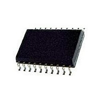
L6201PS STMicroelectronics, L6201PS Datasheet - Page 10

L6201PS
Manufacturer Part Number
L6201PS
Description
IC DRIVER FULL BRIDGE 20-PWRSOIC
Manufacturer
STMicroelectronics
Type
H Bridger
Datasheet
1.L6201013TR.pdf
(20 pages)
Specifications of L6201PS
Input Type
Non-Inverting
Number Of Outputs
2
On-state Resistance
300 mOhm
Current - Output / Channel
4A
Current - Peak Output
5A
Voltage - Supply
12 V ~ 48 V
Operating Temperature
-40°C ~ 150°C
Mounting Type
Surface Mount
Package / Case
PowerSO-20 Exposed Bottom Pad
Operating Supply Voltage
12 V to 48 V
Supply Current
0.015 A
Mounting Style
SMD/SMT
Motor Type
Full Bridge
No. Of Outputs
2
Output Current
5A
Output Voltage
60V
Supply Voltage Range
12V To 48V
Driver Case Style
SOIC
No. Of Pins
20
Operating Temperature Range
-40°C To +150°C
Rohs Compliant
Yes
Operating Current
15mA
Operating Temperature Classification
Automotive
Package Type
PowerSO
Operating Supply Voltage (min)
12V
Operating Supply Voltage (typ)
36V
Operating Supply Voltage (max)
48V
Lead Free Status / RoHS Status
Lead free / RoHS Compliant
Other names
497-1419-5
Available stocks
Company
Part Number
Manufacturer
Quantity
Price
Company:
Part Number:
L6201PS
Manufacturer:
STMicroelectronics
Quantity:
135
Part Number:
L6201PSTR
Manufacturer:
SOIC20
Quantity:
20 000
Company:
Part Number:
L6201PSTR-ST
Manufacturer:
ST
Quantity:
6
L6201 - L6202 - L6203
CIRCUIT DESCRIPTION
The L6201/1PS/2/3 is a monolithic full bridge
switching motor driver realized in the new Mul-
tipower-BCD technology which allows the integra-
tion of multiple, isolated DMOS power transistors
plus mixed CMOS/bipolar control circuits. In this
way it has been possible to make all the control
inputs TTL, CMOS and C compatible and elimi-
nate the necessity of external MOS drive compo-
nents. The Logic Drive is shown in table 1.
Table 1
L = Low
(*) Numbers referred to INPUT1 or INPUT2 controlled output stages
Although the device guarantees the absence of
cross-conduction, the presence of the intrinsic di-
odes in the POWER DMOS structure causes the
generation of current spikes on the sensing termi-
nals. This is due to charge-discharge phenomena
in the capacitors C1 & C2 associated with the
drain source junctions (fig. 14). When the output
switches from high to low, a current spike is gen-
erated associated with the capacitor C1. On the
low-to-high transition a spike of the same polarity
is generated by C2, preceded by a spike of the
opposite polarity due to the charging of the input
capacity of the lower POWER DMOS transistor
(fig. 15).
Figure 14: Intrinsic Structures in the POWER
10/20
V
V
EN
EN
= H
= L
Inputs
DMOS Transistors
H = High
IN1
H
H
X
L
L
IN2
H
H
X
L
L
X = DON’t care
All transistors turned oFF
Sink 1, Sink 2
Sink 1, Source 2
Source 1, Sink 2
Source 1, Source 2
Output Mosfets (*)
Figure 15: Current Typical Spikes on the Sens-
TRANSISTOR OPERATION
ON State
When one of the POWER DMOS transistor is ON
it can be considered as a resistor R
throughout the recommended operating range. In
this condition the dissipated power is given by :
The low R
can provide high currents with low power dissipa-
tion.
OFF State
When one of the POWER DMOS transistor is
OFF the V
age and only the leakage current I
power dissipation during this period is given by :
The power dissipation is very low and is negligible
in comparison to that dissipated in the ON
STATE.
Transitions
As already seen above the transistors have an in-
trinsic diode between their source and drain that
can operate as a fast freewheeling diode in
switched mode applications. During recirculation
with the ENABLE input high, the voltage drop
across the transistor is R
reaches the diode forward voltage it is clamped.
When the ENABLE input is low, the POWER
MOS is OFF and the diode carries all of the recir-
culation current. The power dissipated in the tran-
sitional times in the cycle depends upon the volt-
age-current waveforms and in the driving mode.
(see Fig. 7ab and Fig. 8abc).
DS (ON)
DS
P
ing Pin
ON
P
voltage is equal to the supply volt-
trans.
= R
P
of the Multipower-BCD process
OFF
DS (ON)
= I
= V
DS
(t) V
S
DS (ON)
I
DS
I
DSS
2
DS
(RMS)
(t)
I
DSS
D
and when it
flows. The
DS (ON)


