VN920-B5 STMicroelectronics, VN920-B5 Datasheet - Page 4
VN920-B5
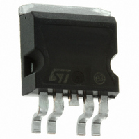
Manufacturer Part Number
VN920-B5
Description
IC DRIVER SINGLE 30A P2-PAK
Manufacturer
STMicroelectronics
Type
High Sider
Specifications of VN920-B5
Input Type
Non-Inverting
Number Of Outputs
1
On-state Resistance
16 mOhm
Current - Output / Channel
45A
Voltage - Supply
5.5 V ~ 36 V
Operating Temperature
-40°C ~ 150°C
Mounting Type
Surface Mount
Package / Case
P²PAK (4 leads + Tab)
Switch Type
High Side
Power Switch Family
VN920
Power Switch On Resistance
16mOhm
Mounting
Surface Mount
Supply Current
10uA
Package Type
P2PAK
Operating Temperature (min)
-40C
Operating Temperature (max)
150C
Operating Temperature Classification
Automotive
Pin Count
4 +Tab
Power Dissipation
96.1W
Supply Voltage (min)
5.5 V
Maximum Power Dissipation
96100 mW
Maximum Operating Temperature
+ 150 C
Mounting Style
SMD/SMT
Minimum Operating Temperature
- 40 C
Current, Output
A
Delay, Propagation, Turn-off
50 us (Typ.) @ 1.3 Ohms
Delay, Propagation, Turn-on
50 us (Typ.) @ 1.3 Ohms
Temperature, Ambient, Maximum
150 °C
Temperature, Ambient, Minimum
-55 °C
Thermal Resistance, Junction To Ambient
51.3 °C⁄W (Max.)
Transistor Type
CMOS
Lead Free Status / RoHS Status
Lead free / RoHS Compliant
Current - Peak Output
-
Lead Free Status / Rohs Status
Not Compliant
Other names
497-2678-5
Available stocks
Company
Part Number
Manufacturer
Quantity
Price
Company:

Part Number:
VN920-B513TR
Manufacturer:
ST
Quantity:
4 500


VN920 / VN920-B5 / VN920SO
ELECTRICAL CHARACTERISTICS (continued)
LOGIC INPUT
Note 1: V
CURRENT SENSE (9V V
Note 2: current sense signal delay after positive input slope.
4/25
R
V
Symbol
I
t
Symbol
V
SENSEO
VSENSEH
dK
dK
dK
DSENSE
V
SENSEH
SENSE
V
V
I(hyst)
K
K
K
V
I
I
1
2
3
IH
ICL
IL
IH
IL
1
/K
2
/K
3
/K
clamp
1
2
3
and V
I
Current Sense Ratio Drift
I
Current Sense Ratio Drift
I
Current Sense Ratio Drift
Analog Sense Leakage
Current
Max Analog Sense Output
Voltage
Sense Voltage in
Overtemperature
conditions
Analog Sense Output
Impedance in
Overtemperature
Condition
Current sense delay
response
Input Low Level
Low Level Input Current
Input High Level
High Level Input Current
Input Hysteresis Voltage
Input Clamp Voltage
OUT
OUT
OUT
OV
/I
/I
/I
SENSE
SENSE
SENSE
are correlated. Typical difference is 5V.
Parameter
Parameter
CC
16V) (See Fig. 1)
V
V
I
I
I
T
I
T
I
T
I
T
I
T
I
T
V
T
V
V
V
V
to 90% I
IN
IN
OUT
OUT
OUT
OUT
OUT
OUT
IN
IN
j
j
j
j
j
j
CC
j
CC
CC
CC
CC
= -40°C...150°C
= -40°C...+150°C
=25°C...150°C
=-40°C...+150°C
=25°C...150°C
=-40°C...+150°C
=-40°C...+150°C
=1mA
=-1mA
=1.25V
=3.25V
=6...16V; I
=5.5V; I
>8V; I
=13V; R
=13V; T
=1A; V
=1A; V
=10A; V
=10A; V
=30A; V
=30A; V
SENSE
OUT
Test Conditions
SENSE
SENSE
OUT
j
SENSE
>T
SENSE
SENSE
SENSE
SENSE
Test Conditions
=10A; R
OUT
(see note 2)
TSD
=5A; R
=0.5V;
=0.5V;
=0A;V
=3.9K
=4V; T
=4V;
=4V; T
=4V;
; Output Open
SENSE
SENSE
SENSE
j
j
=-40°C
=-40°C
=10K
=10K
=0V;
3300
4200
4400
4200
4400
Min
-10
-8
-6
0
2
4
3.25
Min
0.5
1
6
4400
4900
4900
4900
4900
Typ
400
5.5
Typ
-0.7
6.8
Max
6000
6000
5750
5500
5250
+10
500
+8
+6
10
Max
1.25
10
8
Unit
Unit
%
%
%
V
V
V
A
V
V
V
V
V
s
A
A
Related parts for VN920-B5
Image
Part Number
Description
Manufacturer
Datasheet
Request
R

Part Number:
Description:
IC DRIVER SINGLE 30A PENTAWATT
Manufacturer:
STMicroelectronics
Datasheet:

Part Number:
Description:
IC SSR HIGHSIDE 1CH P2PAK-4
Manufacturer:
STMicroelectronics
Datasheet:
Part Number:
Description:
IC DRIVER HIGH SIDE PENTAWATT-5
Manufacturer:
STMicroelectronics
Datasheet:

Part Number:
Description:
IC SSR HIGH SIDE SGL CHAN P2PAK
Manufacturer:
STMicroelectronics
Datasheet:
Part Number:
Description:
IC SSR HIGHSIDE 1CH PENTAWATT5
Manufacturer:
STMicroelectronics
Datasheet:
Part Number:
Description:
IC DRIVER HIGH SIDE PENTAWATT-5
Manufacturer:
STMicroelectronics
Datasheet:
Part Number:
Description:
Single Channel High Side Solid State Relay
Manufacturer:
STMicroelectronics
Datasheet:
Part Number:
Description:
STMicroelectronics [RIPPLE-CARRY BINARY COUNTER/DIVIDERS]
Manufacturer:
STMicroelectronics
Datasheet:
Part Number:
Description:
STMicroelectronics [LIQUID-CRYSTAL DISPLAY DRIVERS]
Manufacturer:
STMicroelectronics
Datasheet:

Part Number:
Description:
BOARD EVAL FOR MEMS SENSORS
Manufacturer:
STMicroelectronics
Datasheet:
Part Number:
Description:
NPN TRANSISTOR POWER MODULE
Manufacturer:
STMicroelectronics
Datasheet:
Part Number:
Description:
TURBOSWITCH ULTRA-FAST HIGH VOLTAGE DIODE
Manufacturer:
STMicroelectronics
Datasheet: