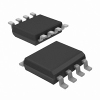
IR2085STRPBF International Rectifier, IR2085STRPBF Datasheet - Page 6

IR2085STRPBF
Manufacturer Part Number
IR2085STRPBF
Description
IC DRIVER HALF BRIDGE OSC 8SOIC
Manufacturer
International Rectifier
Specifications of IR2085STRPBF
Configuration
Half Bridge
Input Type
Self Oscillating
Current - Peak
1A
Number Of Configurations
1
Number Of Outputs
2
High Side Voltage - Max (bootstrap)
100V
Voltage - Supply
10 V ~ 15 V
Operating Temperature
-40°C ~ 125°C
Mounting Type
Surface Mount
Package / Case
8-SOIC (3.9mm Width)
Number Of Drivers
2
Driver Configuration
Self-Oscillating
Driver Type
High and Low Side
Rise Time
60ns
Fall Time
30ns
Frequency (max)
500KHz
Operating Supply Voltage (max)
15V
Peak Output Current
1mA
Power Dissipation
1W
Operating Supply Voltage (min)
10V
Operating Temp Range
-40C to 125C
Operating Temperature Classification
Automotive
Mounting
Surface Mount
Pin Count
8
Package Type
SOIC
Module Configuration
Half Bridge
Input Delay
40ns
Output Delay
20ns
Supply Voltage Range
10V To 15V
Driver Case Style
SOIC
No. Of Pins
8
Rohs Compliant
Yes
Lead Free Status / RoHS Status
Lead free / RoHS Compliant
Delay Time
-
Lead Free Status / Rohs Status
Compliant
Other names
IR2085SPBFTR
Available stocks
Company
Part Number
Manufacturer
Quantity
Price
Company:
Part Number:
IR2085STRPBF
Manufacturer:
International Rectifier
Quantity:
1 950
Part Number:
IR2085STRPBF
Manufacturer:
IR
Quantity:
20 000
IR2085S& (PbF)
Pin Descriptions
Cs: The input pin to the overcurrent comparator. Exceeding the overcurrent threshold value specified in
“Static Electrical Parameters” Section will terminate output pulses and start a new soft start cycle as soon
as the voltage on the pin reduce below the threshold value.
OSC: The oscillator-programming pin. Only two components are required to program the internal oscillator
frequency: a resistor connected between the V
the OSC to COM. The approximate oscillator frequency is determined by the following simple formula:
Where frequency is in Hertz (Hz), RT resistance in Ohms ( ) and CT capacitance in Farads (F). The
recommended range of timing resistors is between 10k
between 47pF and 470pF. The timing resistors less than 10k
capacitor determines the amount of dead time between the two output drivers: lower the CT, shorter the
dead time and vice versa. It is not recommended to use a timing capacitor below 47pF, for best
performance keep the timing components physically as close as possible to the IR2085S. Separated
ground and V
COM: Signal ground and power ground for all functions. Due to high current and high frequency operation,
a low impedance circuit board ground plane is highly recommended.
HO, LO: High side and low side gate drive pins. The high and low side drivers can directly drive the gate
of a power MOSFET. The drivers are capable of 1A peak source and sink currents. It is recommended
that the high and low drive pins be very close to the gates of the high side and low side MOSFETs to
prevent any delay and distortion of the drive signals.
V
low-leakage Schottky diode and a ceramic capacitor. To prevent noise, the Schottky diode and bypass
capacitor should be very close to the IR2085S.
V
side MOSFET with a trace as short as possible.
V
supply current will be higher, depending on the gate charge of the MOSFETs connected to the HO and LO
pins, and the programmed oscillator frequency, total V
the average current at HO and LO. Knowing the operating frequency and the MOSFET gate charge (Qg)
at selected V
Iave = 2 x Qg X f
To prevent noise problem, a bypass ceramic capacitor connected to V
close as possible to the IR2085S.
IR2085S has an under voltage lookout feature for the IC bias supply, V
on V
recommended to prevent asymmetrical gates signal on HO and LO pins that are expected when V
between 7.5V and 8.5V).
6
B
S
CC
: The high side power input connection. The high side supply is derived from a bootstrap circuit using a
: The high side power return connection. V
: The IC bias input connection for the device. Although the quiescent V
CC
to make sure that IC will work within specifications must be higher than 8.5V (9.5V minimum V
f
OSC
= 1 / (2 · R
CC
CC
voltage, the average current can be calculated from:
traces to the timing components are encouraged.
OSC
T
· C
T
)
S
should be connected directly to the source terminal of high
CC
pin and the OSC pin, and a capacitor connected from
CC
current is the sum of quiescent V
and 100k
should be avoided. The value of the timing
and range of time capacitances is
CC
CC
. The minimum voltage required
and COM should be placed as
CC
current is very low, total
CC
current and
www.irf.com
CC
CC
is
is


