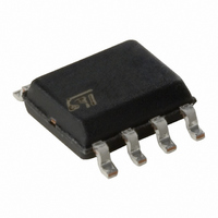
TD352ID STMicroelectronics, TD352ID Datasheet

TD352ID
Specifications of TD352ID
Available stocks
Related parts for TD352ID
TD352ID Summary of contents
Page 1
... Applications ■ 1200V 3-phase inverter ■ Motor control systems ■ UPS Order Codes Part Number Temperature Range TD352IN TD352ID -40°C, +125°C TD352IDT December 2004 Advanced IGBT/MOSFET Driver DIP-8 (Plastic Package) (Plastic Micropackage) Pin Connections (top view) IN VREF TD352 CD ...
Page 2
TD352 1 Block Diagram Figure 1. System and internal block diagram VH 4.7k VREF CD DESAT Table 1. Pin Description Name Pin Number IN 1 Analog input VREF 2 Analog output CD 3 Timing capacitor DESAT 4 Analog input CLAMP ...
Page 3
Absolute Maximum Ratings 2 Absolute Maximum Ratings Table 2. Key parameters and their absolute maximum ratings Symbol VHL Maximum Supply Voltage (VH - VL) Vout Voltage on OUT, CLAMP, LVOFF pins Vter Voltage on other pins (IN, CD, VREF) Pd ...
Page 4
TD352 3 Electrical Characteristics Table -20 to 125°C, VH=16V (unless otherwise specified) amb Symbol Parameter Input Vton IN turn-on threshold voltage Vtoff IN turn-off threshold voltage Iinp IN Input current Voltage reference - Note 1 Vref Voltage ...
Page 5
Functional Description 4 Functional Description 4.1 Input stage TD352 IN input is clamped at about 5V to 7V. The input is triggered by the signal edge. When using an open collector optocoupler, the resistive pull-up resistor can be connected to ...
Page 6
TD352 4.7 Undervoltage protection Undervoltage detection protects the application in the event of a low VH supply voltage (during start- fault situation). During undervoltage, the OUT pin is driven low (active pull-down for VH>2V, passive pull-down for VH<2V. ...
Page 7
Functional Description Figure 3. Detailed internal schematic Comp_Input IN 7V 1V-4V VREF 5V Vref Comp_DelayOff CD 2. 250uA Comp_Desat DESAT VH-2V S1 UVLO Control Block TD352 Comp_Clamp CLAMP 2V VH OUT VL rev. 2 7/13 ...
Page 8
TD352 5 Timing Diagrams Figure 4. General turn-on and turn-off sequence OUT CLAMP Vge VL level Vce Figure 5. input and output waveform dynamic parameters IN (level mode) IN (edge mode) OUT Figure 6. Desaturation fault IN ...
Page 9
Typical Performance Curves 6 Typical Performance Curves Figure 7. Quiescent current vs. temperature 2.5 2.0 1.5 1.0 0.5 0.0 -50 - Temp (°C) Figure 9. Sink current vs. temperature 2000 1800 1600 1400 1200 1000 -50 -25 0 ...
Page 10
TD352 7 Application Diagrams Figure 13. Single supply IGBT drive with active Miller clamp VH 4.7k VREF DESAT Figure 14. Use of DESAT input for direct overcurrent detection VH 4.7k IN VREF Vref CD DESAT Figure 15. Large IGBT drive ...
Page 11
Package Mechanical Data 8 Package Mechanical Data 8.1 DIP-8 Package DIM. MIN 0.7 B 1. 0.44 Plastic DIP-8 MECHANICAL DATA mm. TYP MAX. 3.3 ...
Page 12
TD352 8.2 SO-8 Package DIM. MIN. A 1.35 A1 0.10 A2 1.10 B 0.33 C 0.19 D 4. 5.80 h 0.25 L 0.40 k ddd 12/13 SO-8 MECHANICAL DATA mm. TYP MAX. MIN. 1.75 0.053 0.25 ...
Page 13
... No license is granted by implication or otherwise under any patent or patent rights of STMicroelectronics. Specifications mentioned in this publication are subject to change without notice. This publication supersedes and replaces all information previously supplied. STMicroelectronics products are not authorized for use as critical components in life support devices or systems without express written approval of STMicroelectronics ...


