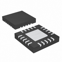
MAX6964ATG+ Maxim Integrated Products, MAX6964ATG+ Datasheet - Page 16

MAX6964ATG+
Manufacturer Part Number
MAX6964ATG+
Description
IC LED DRIVER LINEAR 24-TQFN
Manufacturer
Maxim Integrated Products
Type
Linear (I²C Interface)r
Datasheet
1.MAX6964AEG.pdf
(23 pages)
Specifications of MAX6964ATG+
Topology
Open Drain, PWM
Number Of Outputs
17
Internal Driver
Yes
Type - Primary
Backlight, LED Blinker
Type - Secondary
RGB, White LED
Frequency
400kHz
Voltage - Supply
2 V ~ 3.6 V
Voltage - Output
7V
Mounting Type
Surface Mount
Package / Case
24-TQFN Exposed Pad
Operating Temperature
-40°C ~ 125°C
Current - Output / Channel
50mA
Internal Switch(s)
Yes
Number Of Segments
12
Low Level Output Current
50 mA
Operating Supply Voltage
2 V to 3.6 V
Maximum Supply Current
122.1 uA
Maximum Power Dissipation
1666 mW
Maximum Operating Temperature
+ 125 C
Mounting Style
SMD/SMT
Minimum Operating Temperature
- 40 C
Lead Free Status / RoHS Status
Lead free / RoHS Compliant
Efficiency
-
Lead Free Status / Rohs Status
Details
For example, to operate a 2.2V red LED at 14mA from a
5V supply, R
The MAX6964 can be used to drive loads drawing
more than 50mA, like relays and high-current white
LEDs, by paralleling outputs. Use at least one output
per 50mA of load current; for example, a 6V 330mW
relay draws 55mA and needs two paralleled outputs to
drive it. Ensure that the paralleled outputs chosen are
controlled by the same blink phase register, i.e., select
outputs from the O0 through O7 range, or the O8
through O15 range. This way, the paralleled outputs
are turned on and off together. Do not use output O16
as part of a load-sharing design. O16 cannot be
switched at the same time as any of the other outputs
because it is controlled by a different register.
The MAX6964 must be protected from the negative
voltage transient generated when switching off induc-
tive loads, such as relays, by connecting a reverse-
biased diode across the inductive load (Figure 19). The
peak current through the diode is the inductive load’s
operating current.
17-Output LED Driver/GPO with
Intensity Control and Hot-Insertion Protection
Table 9. PWM Intensity Settings (Blink Disabled)
16
INTENSITY
GLOBAL)
SETTING
OUTPUT
Driving Load Currents Higher than 50mA
(OR
0xA
0xB
0xC
0xD
0x0
0x1
0x2
0x3
0x4
0x5
0x6
0x7
0x8
0x9
0xE
0xF
______________________________________________________________________________________
LED
OUTPUT BLINK PHASE 0
LOW TIME
Static low
PWM DUTY CYCLE
10/16
11/16
12/16
13/16
14/16
15/16
= (5 - 2.2 - 0.25) / 0.014 = 182Ω.
REGISTER BIT = 0
1/16
2/16
3/16
4/16
5/16
6/16
7/16
8/16
9/16
HIGH TIME
Static low
15/16
14/16
13/16
12/16
11/16
10/16
9/16
8/16
7/16
6/16
5/16
4/16
3/16
2/16
1/16
OUTPUT BLINK PHASE 0
LED BEHAVIOR WHEN
Highest PWM intensity
(LED on continuously)
Lowest PWM intensity
Full intensity, no PWM
REGISTER BIT = 0
(LED IS ON WHEN
OUTPUT IS LOW)
Figure 19. Diode-Protected Switching Inductive Load
OUTPUT BLINK PHASE 0
LOW TIME
impedance
0.047µF
Static high
µC
SDA
SCL
PWM DUTY CYCLE
15/16
14/16
13/16
12/16
11/16
10/16
I/O
I/O
9/16
8/16
7/16
6/16
5/16
4/16
3/16
2/16
1/16
REGISTER = 1
2V TO 3.6V
SDA
SCL
BLINK
RST
AD0
V+
HIGH TIME
impedance
Static high
MAX6964
10/16
11/16
12/16
13/16
14/16
15/16
1/16
2/16
3/16
4/16
5/16
6/16
7/16
8/16
9/16
GND
O10
O11
O12
O13
O14
O15
O0
O1
O2
O3
O4
O5
O6
O7
O8
O9
OUTPUT BLINK PHASE 0
LED BEHAVIOR WHEN
Highest PWM intensity
Lowest PWM intensity
LED off continuously
MMTBT4148
REGISTER BIT = 1
(LED IS ON WHEN
OUTPUT IS LOW)
5V


