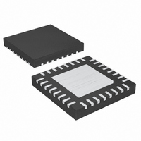
MAX3869ETJ+T Maxim Integrated Products, MAX3869ETJ+T Datasheet - Page 7

MAX3869ETJ+T
Manufacturer Part Number
MAX3869ETJ+T
Description
IC LASER DRIVR 2CHAN 5.5V 32TQFP
Manufacturer
Maxim Integrated Products
Type
Laser Diode Driver (Fiber Optic)r
Datasheet
1.MAX3869EHJ.pdf
(15 pages)
Specifications of MAX3869ETJ+T
Data Rate
2.5Gbps
Number Of Channels
2
Voltage - Supply
3.14 V ~ 5.5 V
Current - Supply
64mA
Current - Modulation
60mA
Current - Bias
100mA
Operating Temperature
-40°C ~ 85°C
Package / Case
32-WFQFN Exposed Pad
Mounting Type
Surface Mount
Lead Free Status / RoHS Status
Lead free / RoHS Compliant
The MAX3869 laser driver consists of two main parts: a
high-speed modulation driver and a laser-biasing block
with automatic power control (APC). The circuit design
is optimized for both high-speed and low-voltage
(+3.3V) operation. To minimize the pattern-dependent
jitter of the input signal at speeds as high as 2.5Gbps,
the device accepts a differential PECL clock signal for
data retiming. When LATCH is high, the input data is
synchronized by the clock signal. When LATCH is low,
the input data is directly applied to the output stage.
The output stage is composed of a high-speed differential
pair and a programmable modulation current source.
Since the modulation output drives a maximum current
of 60mA into the laser with an edge speed of 100ps,
large transient voltage spikes can be generated (due to
the parasitic inductance). These transients and the
laser forward voltage leave insufficient headroom for
the proper operation of the laser driver if the modulation
output is DC-coupled to the laser diode. To solve this
problem, the MAX3869’s modulation output is designed
to be AC-coupled to the cathode of a laser diode. An
external pull-up inductor is necessary to DC-bias the
modulation output at V
laser forward voltage from the output circuitry and
_______________Detailed Description
PIN
20
22
23
24
25
26
27
28
29
30
31
32
_______________________________________________________________________________________
+3.3V, 2.5Gbps SDH/SONET Laser Driver
BIASMAX
MODSET
APCSET
CC
NAME
GND4
GND3
CAPC
GND2
OUT-
V
V
N.C.
MD
CC3
CC2
. Such a configuration isolates
Negative Modulation-Current Output. I
Ground for Output Circuitry
Ground for APC
Monitor Diode Input. Connect this pad to a monitor photodiode anode. A capacitor to ground
is required to filter high-speed AC monitor photocurrent.
Power Supply for APC
A capacitor connected from this pad to ground controls the dominant pole of the APC feed-
back loop (C
Ground for Internal Reference
No Connection. Leave unconnected.
A resistor connected from this pad to ground sets the desired average optical power.
Connect 100kΩ from this pad to ground if APC is not used.
A resistor connected from this pad to ground sets the desired modulation current.
A resistor connected from this pad to ground sets the maximum bias current. The APC
function can subtract from this maximum value, but cannot add to it.
Power Supply for Internal Reference
with Current Monitors and APC
APC
= 0.1µF).
allows the output at OUT+ to swing above and below
the supply voltage V
is shown in Figure 4.
The MAX3869 modulation output is optimized for driv-
ing a 25Ω load; the minimum required voltage at OUT+
is 2.0V. Modulation current swings of 80mA are possi-
ble, but due to minimum power-supply and jitter
requirements at 2.5Gbps, the specified maximum mod-
ulation current is limited to 60mA. To interface with the
laser diode, a damping resistor (R
impedance matching. An RC shunt network may also
be necessary to compensate for the laser-diode para-
sitic inductance, thereby improving the optical output
aberrations and duty-cycle distortion.
At the data rate of 2.5Gbps, any capacitive load at the
cathode of a laser diode will degrade the optical output
performance. Since the BIAS output is directly connect-
ed to the laser cathode, minimize the parasitic capaci-
tance associated with this pin by using an inductor to
isolate the BIAS pin from the laser cathode.
To maintain constant average optical power, the
MAX3869 incorporates an APC loop to compensate for
the changes in laser threshold current over temperature
and lifetime. A back-facet photodiode mounted in the
MOD
FUNCTION
flows through this pad when input data is low.
Pin Description (continued)
CC
Automatic Power Control
. A simplified functional diagram
D
) is required for
7


