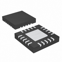
MAX3273ETG+T Maxim Integrated Products, MAX3273ETG+T Datasheet - Page 10

MAX3273ETG+T
Manufacturer Part Number
MAX3273ETG+T
Description
IC LASR DRVR 2.7GBPS 3.6V 24TQFN
Manufacturer
Maxim Integrated Products
Type
Laser Diode Driver (Fiber Optic)r
Datasheet
1.MAX3273ETG.pdf
(18 pages)
Specifications of MAX3273ETG+T
Data Rate
2.7Gbps
Number Of Channels
1
Voltage - Supply
3.14 V ~ 3.6 V
Current - Supply
30mA
Current - Modulation
60mA
Current - Bias
100mA
Operating Temperature
-40°C ~ 85°C
Package / Case
24-TQFN Exposed Pad
Mounting Type
Surface Mount
Lead Free Status / RoHS Status
Lead free / RoHS Compliant
When using the MAX3273 in open-loop operation, the
bias current is determined by the R
select this resistor, see the I
in the Typical Operating Characteristics and select the
value of R
I
loop operation.
When the MAX3273’s APC feature is used, program the
average optical power by adjusting the APCSET resis-
tor. To select this resistor, determine the desired moni-
tor current to be maintained over temperature and life.
See the I
Operating Characteristics and select the value of R
SET
When using the MAX3273 in closed-loop operation, the
R
able to the laser diode over temperature and life. The
APC loop can subtract from this maximum value but
cannot add to it. See the I
in the Typical Operating Characteristics and select the
value of R
bias current at +85°C.
To minimize optical output aberrations caused by sig-
nal reflections at the electrical interface to the laser
diode, a series-damping resistor (R
the Typical Application Circuit ). Additionally, the
MAX3273 outputs are optimized for a 25Ω load.
Therefore, the series combination of R
R
25Ω. Typical values for RD are 18Ω to 23Ω. For best
performance, a bypass capacitor (0.01µF typical)
should be placed as close as possible to the anode of
the laser diode. Depending on the exact characteristics
of the laser diode and PC board layout, a resistor (R
of 50Ω to 100Ω in parallel with pullup inductor L
be useful in damping overshoot and ringing in the opti-
cal output.
In some applications (depending on laser-diode para-
sitic inductance), an RC-shunt network between the
laser cathode and ground helps minimize optical out-
put aberrations. Starting values for most coaxial lasers
are R = 75Ω in series with C = 3.3pF. These values
should be experimentally adjusted until the optical out-
put waveform is optimized.
+3.3V, 2.5Gbps Low-Power Laser Driver
10
BIASMAX
BIASMAX
L
represents the laser-diode resistance) should equal
that corresponds to the required current.
______________________________________________________________________________________
at +25°C. Ground the APCFILT1 pin for open-
resistor sets the maximum bias current avail-
BIASMAX
BIASMAX
MD
vs. R
Programming the Bias Current
Programming the Bias Current
Interfacing with Laser Diodes
that corresponds to the end-of-life
that corresponds to the required
APCSET
BIASMAX
BIASMAX
graph in the Typical
with APC Disabled
with APC Enabled
vs. R
BIASMAX
vs. R
D
) is required (see
D
BIASMAX
BIASMAX
and R
resistor. To
L
(where
P1
graph
graph
APC-
can
P
)
When transmitting NRZ data with long strings of con-
secutive identical digits (CIDs), LF droop can occur
and contribute to pattern-dependent jitter (PDJ). To
minimize this PDJ, three external components must be
properly chosen: capacitor (C
nates the APC loop time constant; pullup inductor (L
and AC-coupling capacitor (C
To filter out noise effects and guarantee loop stability,
the recommended value for C
results in an APC loop bandwidth of 100kHz or a time
constant of 15µs. As a result, the PDJ associated with
an APC loop time constant can be ignored.
The time constant associated with the output pullup
inductor (L
affects the PDJ. For such a second-order network, the
PDJ is dominated by L
cutoff. For a data rate of 2.5Gbps, the recommended
value for C
od, limit the peak voltage droop to less than 12% of the
average (6% of the amplitude). The time constant can
be estimated by:
If τ
7.8µH. To reduce the physical size of this element (L
use of SMD ferrite beads is recommended (Figure 2).
To achieve even greater immunity to droop, use an
optional third inductor (33µH, L
The MAX3273 data and clock inputs are CML compati-
ble. However, it is not necessary to drive the IC with a
standard CML signal. As long as the specified differen-
tial voltage swings are met, the MAX3273 operates
properly.
The junction temperature of the MAX3273 dice must be
kept below +150°C at all times. The total power dissipa-
tion of the MAX3273 can be estimated by the following:
where I
R
typical laser forward voltage.
BIASMAX
LP
P = V
= L
Junction temperature = P(W)
BIAS
, I
P
P
D
CC
MOD
/ 25Ω, and t = 100UI ≈ 40ns, then L
≈ L
is 0.056µF. During the maximum CID peri-
Calculating Power Consumption
is the maximum bias current set by
× I
Input Termination Requirement
P2
is the modulation current, and V
CC
(V
) and the AC-coupling capacitor (C
CC
12
τ
+ (V
LP
%
- 25
Pattern-Dependent Jitter
P
=
CC
because of the low frequency
=
7 8
1
✕
.
- V
−
I
t
MOD
D
P3
e
f
).
APCFILT
)
APCFILT
τ
✕
−
LP
in Figure 2).
t
I
/ 2)
BIAS
✕
37 (°C/W)
), which domi-
is 0.01µF. This
+ I
MOD
✕
f
is the
P
P
P
D
=
);
),
)


