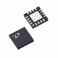
LTC5100EUF#PBF Linear Technology, LTC5100EUF#PBF Datasheet - Page 29

LTC5100EUF#PBF
Manufacturer Part Number
LTC5100EUF#PBF
Description
IC DRIVER VCSEL 3.2GBPS 16QFN
Manufacturer
Linear Technology
Type
Laser Diode Driverr
Datasheet
1.LTC5100EUF.pdf
(52 pages)
Specifications of LTC5100EUF#PBF
Data Rate
3.2Gbps
Number Of Channels
1
Voltage - Supply
3.135 V ~ 3.465 V
Current - Supply
54mA
Current - Modulation
12mA
Operating Temperature
-40°C ~ 85°C
Package / Case
16-QFN
Mounting Type
Surface Mount
Lead Free Status / RoHS Status
Lead free / RoHS Compliant
Available stocks
Company
Part Number
Manufacturer
Quantity
Price
OPERATIO
fault has occurred. For example, the software in the host
system may need to evaluate the cause of the fault before
shutting down the laser. If Auto_shutdn_en = 1, the
LTC5100 automatically disables the transmitter after a
fault. If Auto_shutdn_en = 0, data transmission continues
after a fault. The transmitter is not disabled until the host
system drives the EN pin inactive or clears the Soft_en bit.
Low power supply voltage and memory load errors are
considered hard faults and always disable the transmitter,
regardless of the setting of Auto_shutdn_en.
The LTC5100 implements the GBIC protocol for prevent-
ing software from repeatedly re-enabling a faulted trans-
mitter. When a first fault is detected, it can be cleared by
disabling the transmitter. If the transmitter is re-enabled
and a second fault occurs within 25ms after fault detection
is enabled, the transmitter is permanently disabled. Only
cycling power to the LTC5100 can clear this condition.
This feature is called “Repeated Fault Inhibit” and can be
overridden by setting the Repeated_flt_inhibit bit to zero.
The FAULT pin can be configured active high or active low
with the Flt_pin_polarity bit. The FAULT pin can be pro-
grammed for open drain, 330 A internal pull-up, 500 A
internal pull-up or complementary (push-pull) drive with
the two Flt_drv_mode bits. Refer to Figure 8 for an
equivalent circuit of the FAULT pin.
The FAULT pin can be overridden in software for testing
purposes or to allow a microprocessor in the transceiver
module to fully control the module’s fault output. If the
Flt_pin_override bit is set, then the Force_flt bit fully
controls the state of the FAULT pin.
The state of the LTC5100 can be monitored by reading the
FLT_STATUS register. See Table 21 for a description of the
status bits.
EYE SAFETY INFORMATION
Communications lasers can emit levels of optical power
that pose an eye safety risk. While the LTC5100 provides
certain fault detection features, these features alone do
not ensure that a laser transmitter using the LTC5100 is
compliant with IEC 825 or the regulations of any particu-
lar agency. The user must analyze the safety require-
ments of their transceiver module or system, activate the
U
appropriate laser safety features of the LTC5100, and take
any additional precautions needed to ensure compliance
of the end product with the requirements of the relevant
regulatory agencies. In particular, the LTC5100 produces
laser currents in response to digitally programmed com-
mands. The user must ensure software written to control
the LTC5100 does not cause excessive levels of radiation
to be emitted by the laser.
POWER CONSUMPTION AND POWER MANAGEMENT
The power consumption of the LTC5100 is dependent on
several variables, including the modulation current range
(set by Im_rng), the laser bias and modulation levels, and
the state of the transmitter (whether enabled or disabled.)
If Power_down_en = 1, the LTC5100 turns off its high
speed amplifiers when the transmitter is disabled, reduc-
ing supply current to less than 5mA (typical). See the
Typical Performance Chacteristics for further information.
HIGH SPEED PEAKING CONTROL
The LTC5100 has the ability to selectively peak the falling
edge of the modulation waveform to accelerate the turn-off
of the laser diode. The 5-bit PEAKING register controls this
function. See the Typical Performance Chacteristics for
further information. Lower values in the PEAKING register
increase the falling edge peaking.
ANALOG-TO-DIGITAL CONVERSION
Overview
The ADC in the LTC5100 is a 10-bit, dual slope integrating
converter with excellent linearity and noise rejection. A
multiplexer allows digitizing six quantities:
• SRC pin current, I
• Average modulation current, I
• Laser diode voltage, V
• Monitor diode current, I
• Termination resistor voltage, V
• Die temperature, T
All of these measurements are available to the user via the
I
2
C serial bus.
S
LD
MD
M
TERM
LTC5100
sn5100 5100fs
29


