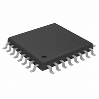
MAX3669EHJ+ Maxim Integrated Products, MAX3669EHJ+ Datasheet - Page 2

MAX3669EHJ+
Manufacturer Part Number
MAX3669EHJ+
Description
IC LASR DRVR 622MBPS 5.5V 32TQFP
Manufacturer
Maxim Integrated Products
Type
Laser Diode Driver (Fiber Optic)r
Datasheet
1.MAX3669EHJ.pdf
(15 pages)
Specifications of MAX3669EHJ+
Data Rate
622Mbps
Number Of Channels
1
Voltage - Supply
3.14 V ~ 5.5 V
Current - Supply
40mA
Current - Modulation
75mA
Current - Bias
80mA
Operating Temperature
-40°C ~ 85°C
Package / Case
32-TQFP, 32-VQFP
Mounting Type
Surface Mount
Lead Free Status / RoHS Status
Lead free / RoHS Compliant
ABSOLUTE MAXIMUM RATINGS
Supply Voltage, V
Current into BIAS ............................................-20mA to +150mA
Current into OUT+, OUT- ............................... -20mA to +100mA
Current into MD....................................................-5mA to +5mA
Voltage at DATA+, DATA-, ENABLE,
Voltage at OUT+, OUT- .............................+1.5V to (V
Voltage at MODSET, APCSET, BIASMAX,
DC ELECTRICAL CHARACTERISTICS
(V
+3.3V, 622Mbps SDH/SONET
Laser Driver with Current Monitors and APC
Stresses beyond those listed under “Absolute Maximum Ratings” may cause permanent damage to the device. These are stress ratings only, and functional
operation of the device at these or any other conditions beyond those indicated in the operational sections of the specifications is not implied. Exposure to
absolute maximum rating conditions for extended periods may affect device reliability.
2
Supply Current
Bias Current Range
Bias Off Current
Bias Current Stability
Bias Current Absolute Accuracy
Differential Input Voltage
Common-Mode Input Voltage
DATA+, DATA- Input Current
Monitor Diode Current Stability
Monitor Diode Current
Absolute Accuracy
DC Monitor Diode Current
BIASMON to I
MODMON to I
Monitor Diode Input Voltage
(MD Pin)
TTL Input High Voltage
TTL Input Low Voltage
TTL Output High Voltage (FAIL)
TTL Output Low Voltage (FAIL)
CC
FAIL, BIASMON, MODMON ..................-0.5V to (V
CAPC............................................................... -0.5V to +3.0V
_______________________________________________________________________________________
= +3.14V to +5.5V, T
PARAMETER
BIAS
MOD
CC
Gain
Gain
.............................................-0.5V to +7.0V
A
= -40°C to +85°C, unless otherwise noted. Typical values are at V
SYMBOL
A
A
I
V
V
V
V
BIAS
I
V
V
MOD
V
BIAS
I
MD
ICM
MD
OH
IN
OL
ID
IH
IL
(Note 2)
V
ENABLE = low (Note 3)
APC open loop
APC open loop
Figure 1
PECL compatible
(Note 4)
I
I
Sourcing 50µA
Sinking 100µA
BIAS
MOD
BIAS
/I
CC
/I
CC
BIASMON
= V
MODMON
+ 0.5V)
+ 1.5V)
CC
- 1.6V
CONDITIONS
Voltage at BIAS .........................................+1.0V to (V
Continuous Power Dissipation (T
Operating Junction Temperature Range ...........-55°C to +150°C
Processing Temperature (Die).........................................+400°C
Storage Temperature Range ............................ -65°C to +165°C
Lead Temperature (soldering, 10s) .................................+300°C
I
I
I
I
BIAS
BIAS
MD
MD
24-Lead Thin QFN
32-Pin TQFP (derate 14.3mW/°C above +85°C).........929mW
(derate 20.8mW/°C above +85°C) ........................1354mW
= 1mA
= 18µA (Note 5)
= 80mA
= 1mA
CC
= +3.3V, T
V
-480
MIN
1.49
200
-15
-15
2.4
0.1
CC
18
-1
1
2
-
A
= +85°C)
V
CC
V
TYP
1.32
A
255
815
-50
0.8
CC
40
35
38
29
= +25°C.) (Note 1)
- 0.3
-
V
V
+480
MAX
1600
1000
V
0.44
+15
+10
+15
100
0.8
CC
60
80
ID
CC
/4
-
CC
ppm/°C
ppm/°C
mA/mA
mA/mA
UNITS
mV
+ 0.5V)
mA
mA
µA
µA
µA
%
%
V
V
V
V
V
V
P-P


