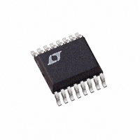
LT4254IGN Linear Technology, LT4254IGN Datasheet - Page 7

LT4254IGN
Manufacturer Part Number
LT4254IGN
Description
IC CTLR HOTSWAP POS 16-SSOP
Manufacturer
Linear Technology
Type
Hot-Swap Controllerr
Datasheet
1.LT4254CGNPBF.pdf
(16 pages)
Specifications of LT4254IGN
Applications
General Purpose
Internal Switch(s)
No
Voltage - Supply
10.8 V ~ 36 V
Operating Temperature
-40°C ~ 85°C
Mounting Type
Surface Mount
Package / Case
16-SSOP (0.150", 3.90mm Width)
Lead Free Status / RoHS Status
Contains lead / RoHS non-compliant
Available stocks
Company
Part Number
Manufacturer
Quantity
Price
Company:
Part Number:
LT4254IGN
Manufacturer:
LT
Quantity:
10 000
Part Number:
LT4254IGN
Manufacturer:
LINEAR/凌特
Quantity:
20 000
Part Number:
LT4254IGN#PBF
Manufacturer:
LINEAR/凌特
Quantity:
20 000
Part Number:
LT4254IGN#TRPBF
Manufacturer:
LINEAR/凌特
Quantity:
20 000
PI FU CTIO S
reaches 4.65V (typ), the GATE pin is pulled low; the TIMER
pull-up current will be turned off and the capacitor is dis-
charged by a 3µA pull-down current. When the TIMER pin
falls below 0.65V (typ), the GATE pin turns on again if the
RETRY pin is high (if the RETRY pin is low, the UV pin must
be pulsed low to reset the internal fault latch before the
GATE pin will turn on). If the RETRY pin is grounded and
the UV pin is not cycled low, the GATE pin remains latched
off and the TIMER pin will be discharged near ground. The
UV pin must be cycled low after the TIMER pin has dis-
charged below 0.65V (typ) to reset the part.
If the RETRY pin is floating or connected to a voltage above
its 1.2V threshold, the LT4254 automatically restarts after
a current fault. Under an output short-circuit condition, the
LT4254 cycles on and off with a 3% on-time duty cycle.
RETRY: Current Fault Retry. RETRY commands the opera-
tional mode of the current limit. If the RETRY pin is
floating, the LT4254 automatically restarts after a current
fault. If it is connected to a voltage below 0.4V, the part
latches off after a current fault (which requires that the UV
pin be cycled low in order to start normal operation again).
GATE: High Side Gate Drive for the External N-Channel
MOSFET. An internal charge pump guarantees at least 10V
of gate drive for V
gate drive for V
The rising slope of the voltage on GATE is set by an external
capacitor connected from the GATE pin to GND and an
internal 35µA pull-up current source from the charge
pump output.
If the current limit is reached, the GATE pin voltage is
adjusted to maintain a constant voltage across the sense
resistor while the timing capacitor starts to charge. If the
TIMER pin voltage ever exceeds 4.65V, the GATE pin is
pulled low.
The GATE pin is also pulled to GND whenever the UV pin
is pulled low, or the V
externally programmed undervoltage threshold or above
the overvoltage threshold.
The GATE pin is clamped internally to a maximum voltage
of 11V (typ) above V
U
U
CC
supply voltages between 10.8V and 20V.
CC
CC
supply voltages above 20V and 4.5V
U
CC
under normal operating conditions.
supply voltage drops below the
Driving this pin beyond the clamp voltage may damage the
part. A zener diode is needed between the gate and source
of the external MOSFET to protect its gate oxide under in-
stantaneous short-circuit conditions. See Applications
Information.
SENSE: Current Limit Sense. A sense resistor is placed in
the supply path between V
circuit regulates the voltage across the sense resistor (V
– SENSE) to 50mV while in current limit when FB is 2V or
higher. If FB drops below 2V, the regulated voltage across
the sense resistor decreases linearly and stops at 15mV
when FB is 0V. The OPEN output also uses SENSE to detect
when the output current is less than (3.5mV)/R5. To defeat
current limit, connect SENSE to V
PWRGD: Open Collector Output to GND. PWRGD is pulled
low whenever the voltage on FB falls below the high-to-low
threshold voltage. It goes into a high impedance state
when the voltage on FB exceeds the low-to-high threshold
voltage. An external pull-up resistor can pull PWRGD to a
voltage higher or lower than V
this pin and connect FB to the output voltage.
UV: Undervoltage Sense. UV is an input that enables the
output voltage. When the UV pin is driven above 4V, the
GATE pin starts charging and the output turns on. When
the UV pin goes below 3.6V, the GATE pin discharges and
the output shuts off.
Pulsing the UV pin to ground after a current limit fault cycle
(TIMER pin dischaged to below 0.65V typ) resets the fault
latch (when RETRY pin is low, commanding latch off
operation) and allows the part to turn back on. To disable
UV sensing, connect the pin to V
OV: Overvoltage Sense. OV is an input that disables the
output voltage. If OV ever goes above 4V, the GATE pin is
discharged and the output shuts off. When OV goes below
3.6V, the GATE pin starts charging and the output turns
back on. To disable OV sensing, connect pin to ground.
OPEN: Open Circuit Detect Output. This pin is an open
collector output that releases and is pulled high through an
external resistor if the load current is less than (3.5mV/R5).
If not used, leave this pin disconnected.
CC
and SENSE. The current limit
CC
. To disable PWRGD, float
CC
CC
through a 10k resistor.
.
LT4254
4254fb
7
CC


