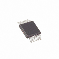
MAX5924DEUB+ Maxim Integrated Products, MAX5924DEUB+ Datasheet - Page 14

MAX5924DEUB+
Manufacturer Part Number
MAX5924DEUB+
Description
IC HOT-SWAP CTRLR N-CH 10-UMAX
Manufacturer
Maxim Integrated Products
Type
Hot-Swap Controllerr
Datasheet
1.MAX5925AEUB.pdf
(21 pages)
Specifications of MAX5924DEUB+
Applications
General Purpose
Internal Switch(s)
No
Voltage - Supply
1 V ~ 13.2 V
Operating Temperature
-40°C ~ 85°C
Mounting Type
Surface Mount
Package / Case
10-MSOP, Micro10™, 10-uMAX, 10-uSOP
Lead Free Status / RoHS Status
Lead free / RoHS Compliant
UVLO circuitry prevents the MAX5924/MAX5925/
MAX5926 from turning on the external MOSFET until V
exceeds the UVLO threshold, V
protects the external MOSFET from insufficient gate-drive
voltage, and t
plugged into the backplane and V
powering the hot-swapped system. Any input voltage
transient at V
the UVLO deglitch period, t
tiates a startup sequence. Device operation is protected
from momentary input-voltage steps extending below the
UVLO threshold for a deglitch period, t
power-good output(s) may momentarily deassert if the
magnitude of a negative step in V
mately 0.5V, and V
unaffected and the power-good output(s) assert(s) within
200µs as shown in Figure 8b. This figure also shows that
if the UVLO condition exceeds t
power-good output(s) again deassert(s) and the load is
disconnected.
Determining a circuit’s inrush current is necessary to
choose a proper MOSFET. The MAX5924/MAX5925/
MAX5926 regulate the inrush current by controlling the
output-voltage slew rate, but inrush current is also a
function of load capacitance. Determine an anticipated
inrush current using the following equation:
1V to 13.2V, n-Channel Hot-Swap Controllers
Require No Sense Resistor
Figure 8b. PGOOD Behavior with Large Negative Input-Voltage
Step when V
14
______________________________________________________________________________________
PGOOD
GATE
V
CC
S
is Near V
CC
D,UVLO
below the UVLO threshold for more than
Undervoltage Lockout (UVLO)
CC
Determining Inrush Current
S(MIN)
drops below V
ensures that the board is fully
200µs/div
DG
, resets the device and ini-
UVLO
DG
CC
CC
, for t
UVLO
= 900µs (typ), the
exceeds approxi-
DG.
is stable prior to
D,UVLO
. Operation is
However, the
2V/div
1V/div
1V/div
. UVLO
CC
where C
selected MAX5924/MAX5925/MAX5926 output slew rate
in V/ms. For example, assuming a load capacitance of
100µF and using the value of SR = 10V/ms, the anticipat-
ed inrush current is 1A. If a 16V/ms output slew rate is
used, the inrush current increases to 1.6A. Choose SR
so the maximum anticipated inrush current does not trip
the fast circuit-breaker comparator during startup.
The MAX5924/MAX5925/MAX5926 limit the slew rate of
V
SLEW and GND to adjust the slew-rate limit. Floating
SLEW sets the maximum slew rate to the minimum value.
Calculate C
where, SR is the desired slew rate in V/ms and C
is in nF.
This equation is valid for C
SR, see the Typical Operating Characteristics .
A 2µA (typ) pullup current clamped to 1.4V causes an
initial jump in the gate voltage, V
and the slew rate is slow (Figure 3). Figure 9 illustrates
how the addition of gate capacitance minimizes this ini-
tial jump. C
Figure 9. Impact of C
OUT
. Connect an external capacitor, C
I
INRUSH
L
is the load capacitance in µF and SR is the
GATE
SLEW
V
C
C
( ) =
S
SLEW
L
A
C
= V
= 10µF
should not exceed 25nF.
using the following equation:
SLEW
GATE
CC
MOSFET ONLY
= 1µF
= 13.2V
C
on the V
L
= 330
10ms/div
dt
dV
×
SLEW
GATE
OUT
1000
10
GATE
Waveform
-9
MOSFET AND
C
≥ 100nF. For higher
GATE
/ SR
=
, if C
= 20nF
C
L
SLEW
GATE
Slew Rate
×
5V/div
0V
0V
SR
, between
is small
SLEW


