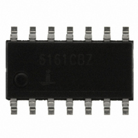
ISL6161CBZA Intersil, ISL6161CBZA Datasheet - Page 3

ISL6161CBZA
Manufacturer Part Number
ISL6161CBZA
Description
IC CTLR PWR DISTRIB DUAL 14SOIC
Manufacturer
Intersil
Type
Hot-Swap Controllerr
Datasheet
1.ISL6161CBZA-T.pdf
(11 pages)
Specifications of ISL6161CBZA
Applications
General Purpose, PCI Express
Internal Switch(s)
No
Voltage - Supply
10.5 V ~ 13.2 V
Operating Temperature
0°C ~ 70°C
Mounting Type
Surface Mount
Package / Case
14-SOIC (0.154", 3.90mm Width)
Peak Reflow Compatible (260 C)
Yes
Rohs Compliant
Yes
Lead Free Status / RoHS Status
Lead free / RoHS Compliant
Available stocks
Company
Part Number
Manufacturer
Quantity
Price
Company:
Part Number:
ISL6161CBZA
Manufacturer:
Intersil
Quantity:
100
Pin Descriptions
PIN NUMBER SYMBOL
10
12
13
14
11
1
2
3
4
5
6
7
8
9
12VISEN 12V Current Sense
ENABLE Enable/Reset
PGOOD
3VISEN
C
12VG
12VS
R
C
GND
V
3VG
3VS
PUMP
NC
ILIM
TIM
DD
12V Source
12V Gate
Chip Supply
Not Connected
3V Gate
3 Source
3V Current Sense
Power-Good indicator Indicates that all output voltages are within specification. PGOOD is driven by an open drain
Current Limit Timing
Capacitor
Charge Pump
Capacitor
Chip Ground
Current Limit Set
Resistor
3
FUNCTION
Connect to source of associated external N-Channel MOSFET switch to sense output
voltage.
Connect to the gate of associated N-Channel MOSFET switch. A capacitor from this node to
ground sets the turn-on ramp. At turn-on this capacitor will be charged to ~17.4V by a 10µA
current source.
Connect to 12V supply. This can be either connected directly to the +12V rail supplying the
load voltage or to a dedicated V
V
ENABLE is used to turn-on and reset the chip. Both outputs turn-on when this pin is driven
low. After a current limit time-out, the chip is reset by the rising edge of a reset signal applied
to the ENABLE pin. This input has 100µA pull-up capability, which is compatible with 3V and
5V open drain and standard logic.
Connect to the gate of the external 3V N-Channel MOSFET. A capacitor from this node to
ground sets the turn-on ramp. At turn-on, this capacitor will be charged to ~11.4V by a 10µA
current source.
Connect to the source side of 3V external N-Channel MOSFET switch to sense output
voltage.
Connect to the load side of the 3V sense resistor to measure the voltage drop across this
resistor between 3VS and 3VISEN pins.
N-Channel MOSFET. It is pulled low when any output is not within specification.
Connect a capacitor from this pin to ground. This capacitor controls the time between the
onset of current limit and chip shutdown (current limit time-out). The duration of current limit
time-out (in seconds) = 200kΩ x C
Connect a 0.1µF capacitor between this pin and V
12VG drive.
A resistor connected between this pin and ground determines the current level at which
current limit is activated. This current is determined by the ratio of the R
sense resistor (R
10µA x (R
resistor whereas the ISL6161 can accommodate a 5kΩ resistor for a lower OC Vth (50mV).
Connect to the load side of sense resistor to measure the voltage drop across this resistor.
DD
decoupling must be paid to prevent sagging as heavy loads are switched on.
ILIM
ISL6161
/R
SENSE
SENSE
). The ISL6161 is limited to a 10kΩ min. value (OC Vth = 100mV)
). The current at current limit onset is equal to
DD
TIM
+12V supply. If the former is chosen, special attention to
DESCRIPTION
(Farads).
DD
(pin 3). Provides charge storage for
ILIM
resistor to the
October 2, 2008
FN9104.4


