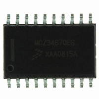
MCZ34670EG Freescale Semiconductor, MCZ34670EG Datasheet - Page 14

MCZ34670EG
Manufacturer Part Number
MCZ34670EG
Description
IC POE CURR MODE SW REG 20-SOIC
Manufacturer
Freescale Semiconductor
Type
Power Over Ethernet Controller (PoE)r
Datasheet
1.MCZ34670EGR2.pdf
(24 pages)
Specifications of MCZ34670EG
Applications
Remote Peripherals (Industrial Controls, Cameras, Data Access)
Internal Switch(s)
No
Voltage - Supply
60V
Operating Temperature
-40°C ~ 85°C
Mounting Type
Surface Mount
Package / Case
20-SOIC (0.300", 7.50mm Width)
Product
PoE / LAN Solutions
Supply Voltage (max)
80 V
Supply Voltage (min)
- 0.3 V
Power Dissipation
800 mW
Operating Temperature Range
- 40 C to + 85 C
Mounting Style
SMD/SMT
Supply Current
18 mA
Output Current
2.1A
Digital Ic Case Style
SOIC
No. Of Pins
20
Duty Cycle (%)
48%
Uvlo
2V
Frequency
400kHz
Msl
MSL 3 - 168 Hours
Rohs Compliant
Yes
Lead Free Status / RoHS Status
Lead free / RoHS Compliant
Available stocks
Company
Part Number
Manufacturer
Quantity
Price
Part Number:
MCZ34670EG
Manufacturer:
FREESCALE
Quantity:
20 000
Company:
Part Number:
MCZ34670EGR2
Manufacturer:
KODENSHI
Quantity:
6 400
signature resistor, the total resistance of R
25 kΩ.
be connected to VIN. In this case, a valid signature resistor
has to be placed between -V
configuration can be seen in
equations should be used:
where V
V
CURRENT-MODE CONTROL OPERATION
leading-edge blanking. The current-limit comparator monitors
the CS pin at all times and provides cycle-by-cycle current
limit.
result of the MOSFET gate charge current, capacitive and
14
34670
FUNCTIONAL DEVICE OPERATION
OPERATIONAL MODES
UVLO(ref)
To use the default settings for UVLO, the pin UVLO must
To calculate the values for R
The 34670 offers current-mode control operation with
The CS signal contains a leading-edge spike that is the
UVLO(ON)
Figure 13. UVLO Adjustment by External
the UVLO reference voltage.
Figure 14. Default UVLO Settings
is the desired turn-on voltage threshold and
R 2
+V
-V
+V
-V
PORT
PORT
PORT
PORT
=
Resistor Divider
R 1
V
--------------------------------- - R
V
+
UVLO REF
UVLO ON
R 2
R
25kΩ
SIG
PORT
Figure
(
R
R
=
1
(
1
2
and R
R
and +V
SIG
)
)
14.
⋅
PULSE WITH MODULATOR CONTROLLER
VPWR
RCLA
UVLO
ILIM
VIN
2
VPWR
RCLA
UVLO
ILIM
VIN
SIG
the following
PORT
1
+R
. This
2
must equal
on voltage V
INRUSH CURRENT LIMITATION
PoE-PSEs which do not meet the inrush current requirement
of the IEEE 802.3af specification. By setting the initial inrush
current limit to a low level, a PD using the 34670 minimizes
the current drawn from the PSE during start-up. The
maximum inrush current level can be set by connecting a
resistor from ILIM to V
the corresponding resistor value that has to be connected
between pins ILIM and VIN:
Table 9. Inrush Current Limit vs. R
current limit, thereby allowing the PD to consume up to
12.95 W if a 802.3af PSE is present.
diode reverse recovery current of the power circuit. The
leading-edge blanking of the CS signal prevents the PWM
comparator from premature termination of the on cycle.
advantageous for applications which are not allowed to
exceed an on-time of 50 % of the switching period T
the duty-cycle limit, slope compensation is provided to
stabilize the inner current loop and avoid oscillations for
The typical turn-off voltage V
The 34670 has been designed to interface also with legacy
The following table shows the selectable current limits and
After powering up, the 34670 switches to the high level
The 34670 limits the duty cycle to 50%. This is
Inrush Current Limit [mA]
Figure 15. Inrush Current Limitation by External
+V
UVLO(ON)
-V
V
180
110
PORT
PORT
65
UVLO OFF
(
.
R
25kΩ
R 1
IN
SIG
Analog Integrated Circuit Device Data
Resistor R
as illustrated in
)
=
=
R
V
SIG
R
UVLO ON
R
CLASS
UVLO(OFF)
ILIM
–
ILIM
Freescale Semiconductor
R 2
(
ILIM
R
ILIM
)
Figure
VPWR
RCLA
UVLO
ILIM
VIN
⋅
is 85% of the turn
0.85
Value [kΩ]
12.1
42.2
191
15.
S
. Beside


