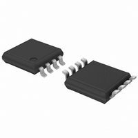
PCA9512ADP,118 NXP Semiconductors, PCA9512ADP,118 Datasheet - Page 12

PCA9512ADP,118
Manufacturer Part Number
PCA9512ADP,118
Description
IC LEVSHFT I2C/SMBUS BUFF 8TSSOP
Manufacturer
NXP Semiconductors
Type
I²C-Bus and SMBus Switchr
Specifications of PCA9512ADP,118
Package / Case
8-TSSOP
Applications
Hot-Swap/SMB Buffer
Internal Switch(s)
Yes
Voltage - Supply
2.7 V ~ 5.5 V
Operating Temperature
-40°C ~ 85°C
Mounting Type
Surface Mount
Logic Family
PCA
Maximum Operating Temperature
85 C
Mounting Style
SMD/SMT
Minimum Operating Temperature
- 40 C
Number Of Lines (input / Output)
3 / 3
Logic Type
Bus Buffer
Operating Temperature (min)
-40C
Operating Temperature Classification
Industrial
Operating Temperature (max)
85C
Package Type
TSSOP
Rad Hardened
No
Lead Free Status / RoHS Status
Lead free / RoHS Compliant
Lead Free Status / RoHS Status
Lead free / RoHS Compliant, Lead free / RoHS Compliant
Other names
568-3362-2
935279719118
PCA9512ADP-T
935279719118
PCA9512ADP-T
NXP Semiconductors
11. Characteristics
Table 5.
V
PCA9512A_PCA9512B
Product data sheet
Symbol
Power supply
V
V
I
I
Start-up circuitry
V
t
t
Rise time accelerators
I
V
V
I
t
Input-output connection
V
C
V
I
CC
CC2
en
idle
trt(pu)
I(ACC)
PD(on/off)(ACC)
LI
CC
CC
CC2
pch
th(dis)(ACC)
th(en)(ACC)
offset
OL
i
= 2.7 V to 5.5 V; T
Characteristics
Parameter
supply voltage
supply voltage 2
supply current
supply current 2
precharge voltage
enable time
idle time
transient boosted pull-up
current
disable threshold voltage
on pin ACC
enable threshold voltage
on pin ACC
input current on pin ACC
on/off propagation delay
on pin ACC
offset voltage
input capacitance
LOW-level output voltage
input leakage current
amb
=
−
40
[2]
°
C to +85
All information provided in this document is subject to legal disclaimers.
°
C; unless otherwise specified.
Conditions
V
V
V
V
SDA, SCL floating
on power-up
positive transition on SDA,
SCL; V
V
slew rate = 1.25 V/μs
10 kΩ to V
V
V
digital; guaranteed by design,
not subject to test
V
I
V
SDAn, SCLn pins;
V
sink
CC
SDAIN
CC
SDAOUT
CC
CC
I
I
CC2
CC
= 0.2 V
= 0 V; SDAn, SCLn pins;
= 3 mA; V
= 5.5 V;
= 5.5 V;
= 2.7 V;
= 3.3 V; V
= 5.5 V; V
Rev. 5 — 5 January 2011
= 2.7 V
ACC
= V
Level shifting hot swappable I
= V
CC
SCLIN
= 0.7 × V
SCLOUT
on SDA, SCL;
CC
CC2
CC2
= 0 V
= 2.7 V;
= 3.3 V;
= 5.5 V
= 0 V
CC2
;
PCA9512A; PCA9512B
[1][4]
[5][6]
[1][7]
[1]
[1]
[1]
[3]
[1]
Min
2.7
2.7
-
-
0.8
-
50
1
0.3V
-
−1
-
0
-
0
−1
CC2
2
C-bus and SMBus bus buffer
Typ
-
-
1.8
1.7
1.1
180
140
2
0.5V
0.5V
±0.1
5
115
-
0.3
-
CC2
CC2
© NXP B.V. 2011. All rights reserved.
Max
5.5
5.5
3.6
2.9
1.2
-
250
-
-
0.7V
+1
-
175
10
0.4
+1
CC2
12 of 24
Unit
V
V
mA
mA
V
μs
μs
mA
V
V
μA
ns
mV
pF
V
μA


