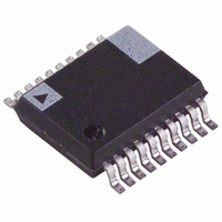
ADE7763ARS Analog Devices Inc, ADE7763ARS Datasheet - Page 21

ADE7763ARS
Manufacturer Part Number
ADE7763ARS
Description
IC ENERGY METER 1PHASE 20SSOP
Manufacturer
Analog Devices Inc
Specifications of ADE7763ARS
Input Impedance
390 KOhm
Measurement Error
0.1%
Voltage - I/o High
2.4V
Voltage - I/o Low
0.8V
Current - Supply
3mA
Voltage - Supply
4.75 V ~ 5.25 V
Operating Temperature
-40°C ~ 85°C
Mounting Type
Surface Mount
Package / Case
20-SSOP (0.200", 5.30mm Width)
Meter Type
Single Phase
For Use With
EVAL-ADE7763ZEB - BOARD EVALUATION FOR ADE7763
Lead Free Status / RoHS Status
Contains lead / RoHS non-compliant
Available stocks
Company
Part Number
Manufacturer
Quantity
Price
Part Number:
ADE7763ARS
Manufacturer:
ADI/亚德诺
Quantity:
20 000
Part Number:
ADE7763ARSZ
Manufacturer:
ADI/亚德诺
Quantity:
20 000
Part Number:
ADE7763ARSZRL
Manufacturer:
ADI/亚德诺
Quantity:
20 000
Channel 1 Sampling
The waveform samples may be routed to the waveform register
(MODE[14:13] = 1, 0) for the system master (MCU) to read. In
waveform sampling mode, set the WSMP bit (Bit 3) in the
interrupt enable register to Logic 1. The active and apparent
power as well as the energy calculation remain uninterrupted
during waveform sampling.
In waveform sampling mode, choose one of four output sample
rates using Bits 11 and 12 of the mode register (WAVSEL 1, 0).
The output sample rate can be 27.9 kSPS, 14 kSPS, 7 kSPS, or
3.5 kSPS—see the Mode Register (0X09) section. The interrupt
request output, IRQ , signals a new sample availability by going
active low. The timing is shown in
form samples are transferred from the ADE7763 one byte (eight
bits) at a time, with the most significant byte shifted out first.
The 24-bit data-word is right justified—see the
section. The interrupt request output
interrupt routine reads the reset status register—see the
Interrupts
DOUT
SCLK
IRQ
DIN
0.5V, 0.25V,
0.125V, 62.5mV,
31.3mV, 15.6mV,
section.
READ FROM WAVEFORM
Figure 44. Waveform Sampling Channel 1
0
0 0 01 HEX
0V
V1
*WHEN DIGITAL INTEGRATOR IS ENABLED, FULL-SCALE OUTPUT DATA IS ATTENUATED
DEPENDING ON THE SIGNAL FREQUENCY BECAUSE THE INTEGRATOR HAS A –20dB/DECADE
FREQUENCY RESPONSE. WHEN DISABLED, THE OUTPUT IS NOT ATTENUATED FURTHER.
ANALOG
INPUT
RANGE
V1
V1P
V1N
SIGN
PGA1
Figure 44
×1, ×2, ×4,
×8, ×16
{GAIN[2:0]}
IRQ stays low until the
0x28 51EC
0xD 7AE4
CHANNEL 1 DATA
0x0 0000
(24 BITS)
2.42V, 1.21V, 0.6V
. The 24-bit wave-
REFERENCE
ADC 1
Serial Interface
Figure 43. ADC and Signal Processing in Channel 1
ADC OUTPUT
WORD RANGE
{GAIN[4:3]}
Rev. B | Page 21 of 56
HPF
0x28 51EC
0x00 0000
0xD 7AE4
INTEGRATOR*
DIGITAL
Channel 1 RMS Calculation
The root mean square (rms) value of a continuous signal V(t) is
defined as
For time sampling signals, the rms calculation involves squaring
the signal, taking the average, and obtaining the square root:
The ADE7763 simultaneously calculates the rms values for
Channel 1 and Channel 2 in different registers. Figure 45 shows
the detail of the signal processing chain for the rms calculation
on Channel 1. The Channel 1 rms value is processed from the
samples used in the Channel 1 waveform sampling mode. The
Channel 1 rms value is stored in an unsigned, 24-bit register
(IRMS). One LSB of the Channel 1 rms register is equivalent to
1 LSB of a Channel 1 waveform sample. The update rate of the
Channel 1 rms measurement is CLKIN/4.
CHANNEL 1
(CURRENT WAVEFORM)
DATA RANGE
dt
VRMS =
VRMS =
T
N
1
1
×
×
T
∫
0
∑
i
N
V
=
1
V
2
50Hz
0x1E F73C
) (
0x19 CE08
0xE6 31F8
0x00 0000
0x00 0000
0xEI 08C4
2
t
) (
dt
i
60Hz
CURRENT RMS (IRMS)
CALCULATION
WAVEFORM SAMPLE
REGISTER
ACTIVE AND REACTIVE
POWER CALCULATION
CHANNEL 1
(CURRENT WAVEFORM)
DATA RANGE AFTER
INTEGRATOR (50Hz)
CHANNEL 1
(CURRENT WAVEFORM)
DATA RANGE AFTER
INTEGRATOR (60Hz)
ADE7763
(2)
(3)


