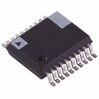
ADE7753ARS Analog Devices Inc, ADE7753ARS Datasheet - Page 27

ADE7753ARS
Manufacturer Part Number
ADE7753ARS
Description
IC ENERGY METERING DETEC 20-SSOP
Manufacturer
Analog Devices Inc
Specifications of ADE7753ARS
Rohs Status
RoHS non-compliant
Input Impedance
390 KOhm
Measurement Error
0.1%
Voltage - I/o High
2.4V
Voltage - I/o Low
0.8V
Current - Supply
3mA
Voltage - Supply
4.75 V ~ 5.25 V
Operating Temperature
-40°C ~ 85°C
Mounting Type
Surface Mount
Package / Case
20-SSOP (0.200", 5.30mm Width)
Meter Type
Single Phase
For Use With
EVAL-ADE7753ZEB - BOARD EVALUATION AD7753
Available stocks
Company
Part Number
Manufacturer
Quantity
Price
Part Number:
ADE7753ARS
Manufacturer:
ADI/亚德诺
Quantity:
20 000
Part Number:
ADE7753ARSZ
Manufacturer:
ADI/亚德诺
Quantity:
20 000
Part Number:
ADE7753ARSZRL
Manufacturer:
ADI/亚德诺
Quantity:
20 000
CLKIN FREQUENCY
In this datasheet, the characteristics of the ADE7753 is shown
with CLKIN frequency equals 3.579545 MHz. However, the
ADE7753 is designed to have the same accuracy at any
CLKIN frequency within the specified range. If the CLKIN
frequency is not 3.579545MHz, various timing and filter
characteristics will need to be redefined with the new CLKIN
frequency. For example, the cut-off frequencies of all digital
filters (LPF1, LPF2, HPF1, etc.) will shift in proportion to
the change in CLKIN frequency according to the following
equation:
New
The change of CLKIN frequency does not affect the timing
characteristics of the serial interface because the data transfer
is synchronized with serial clock signal (SCLK). But one
needs to observe the read/write timing of the serial data
transfer-see ADE7753 Timing Characteristics.
various timing changes that are affected by CLKIN fre-
quency.
Parameter
Nyquist frequency for CH 1&2 ADCs
PHCAL resolution (seconds per LSB)
Active Energy register update rate (Hz)
Waveform sampling rate (Number of samples per second)
Maximum ZXTOUT period
SUSPENDING THE ADE7753 FUNCTIONALITY
The analog and the digital circuit can be suspended sepa-
rately. The analog portion of the ADE7753 can be suspended
by setting the ASUSPEND bit (bit 4) of the Mode register
to logic high
waveform samples from the ADCs will be set to zeros. The
digital circuitry can be halted by stopping the CLKIN input
and maintaining a logic high or low on CLKIN pin. The
ADE7753 can be reactivated by restoring the CLKIN input
and setting the ASUSPEND bit to logic low.
REV. PrF 10/02
WAVSEL 1,0 =
Frequency
Frequency dependencies of the ADE7753 parameters
Original
See Mode Register. In suspend mode, all
0
0
1
1
Frequency
Table III
0
1
0
1
PRELIMINARY TECHNICAL DATA
CLKIN
. 3
CLKIN dependency
579545
Frequency
C LKIN /8
4/C LKIN
C LKIN /4
CLKIN/128
CLKIN/256
CLKIN/512
CLKIN/1024
524,288/CLKIN
MHz
Table III lists
(27)
–27–
CHECKSUM REGISTER
The ADE7753 has a Checksum register (CHECKSUM[5:0])
to ensure the data bits received in the last serial read operation
are not corrupted. The 6-bit Checksum register is reset
before the first bit (MSB of the register to be read) is put on
the DOUT pin. During a serial read operation, when each
data bit becomes available on the rising edge of SCLK, the
bit will be added to the Checksum register. In the end of the
serial read operation, the content of the Checksum register
will equal to the sum of all ones in the register previously
read. Using the Checksum register, the user can determine
if an error has occured during the last read operation.
Note that a read to the Checksum register will also generate
a checksum of the Checksum register itself.
DOUT
Figure 48– Checksum register for Serial Interface Read
+
+
CONTENT OF REGISTER (n-bytes)
CHECKSUM REGISTER
ADE7753
ADDR: 3Eh


