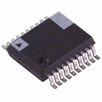
ADE7753ARS Analog Devices Inc, ADE7753ARS Datasheet - Page 32

ADE7753ARS
Manufacturer Part Number
ADE7753ARS
Description
IC ENERGY METERING DETEC 20-SSOP
Manufacturer
Analog Devices Inc
Specifications of ADE7753ARS
Rohs Status
RoHS non-compliant
Input Impedance
390 KOhm
Measurement Error
0.1%
Voltage - I/o High
2.4V
Voltage - I/o Low
0.8V
Current - Supply
3mA
Voltage - Supply
4.75 V ~ 5.25 V
Operating Temperature
-40°C ~ 85°C
Mounting Type
Surface Mount
Package / Case
20-SSOP (0.200", 5.30mm Width)
Meter Type
Single Phase
For Use With
EVAL-ADE7753ZEB - BOARD EVALUATION AD7753
Available stocks
Company
Part Number
Manufacturer
Quantity
Price
Part Number:
ADE7753ARS
Manufacturer:
ADI/亚德诺
Quantity:
20 000
Part Number:
ADE7753ARSZ
Manufacturer:
ADI/亚德诺
Quantity:
20 000
Part Number:
ADE7753ARSZRL
Manufacturer:
ADI/亚德诺
Quantity:
20 000
ADE7753
Address Name
ADE7753 REGISTER DESCRIPTIONS
All ADE7753 functionality is accessed via the on-chip registers. Each register is accessed by first writing to the
communications register and then transferring the register data. A full description of the serial interface protocol is given in
the Serial Interface section of this data sheet.
Communications Register
The Communications register is an 8-bit, write-only register which controls the serial data transfer between the ADE7753
and the host processor. All data transfer operations must begin with a write to the communications register. The data written
to the communications register determines whether the next operation is a read or a write and which register is being accessed.
Table IV below outlines the bit designations for the Communications register.
Bit
Location
0 to 5
6
7
21h
24h
25h
27h
28h-
3Ch
3Dh
3Eh
3Fh
22h
23h
26h
VPKLVL
IPEAK
RSTIPEAK
VPEAK
RSTVPEAK
TEMP
PERIOD
T M O D E
C H K S U M
DIEREV
Bit
Mnemonic
A0 to A5
RESERVED
W/ R
W/R
DB7
R/W
R/W 8 bits
R
R
R
R
R
R
R/W 8 bits
R
R
PRELIMINARY TECHNICAL DATA
DB6
# of Bits
24 bits
24 bits
24 bits
24 bits
8 bits
15 bits
6 bits
8 bits
Description
The six LSBs of the Communications register specify the register for the data transfer
operation. Table III lists the address of each ADE7753 on-chip register.
This bit is unused and should be set to zero.
When this bit is a logic one the data transfer operation immediately following the write to
the Communications register will be interpreted as a write to the ADE7753. When this bit
is a logic zero the data transfer operation immediately following the write to the
Communications register will be interpreted as a read operation.
0
DB5
A5
Table V. Communications Register
Default
F F h
0h
0h
0h
0h
0h
0h
-
0h
-
DB4
A4
Description
Channel 2 Peak Level threshold (voltage channel). This register
sets the level of the voltage peak detection. If the channel 2 input
exceeds this level, the PKV flag in the status register is set.
Channel 1 peak register. The maximum input value of the
Current channel since the last read of the register is stored in this
register.
Same as Channel 1 peak register except that the register contents
are reset to 0 after read.
Channel 2 peak register. The maximum input value of the
Voltage channel since the last read of the register is stored in this
register.
Same as Channel 2 peak register except that the register contents
are reset to 0 after a read.
Temperature register. This is an 8-bit register which contains the
result of the latest temperature conversion – see Temperature
Measurement.
Period of the channel 2 (volatge channel) input estimated by
Zero-crossing processing.
Reserved
Test mode register
Checksum Register.
sum of all the ones in the previous read – see ADE7753 Serial Read
Operation.
Die Revision Register.
revision number of the silicon.
–32–
DB3
A3
DB2
A2
This 6-bit read only register is equal to the
This 8-bit read only register contains the
DB1
A1
DB0
A0
REV. PrF 10/02


