MCP3909-I/SS Microchip Technology, MCP3909-I/SS Datasheet - Page 3
MCP3909-I/SS
Manufacturer Part Number
MCP3909-I/SS
Description
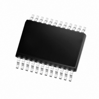
IC POWER METERING-1 PHASE 24SSOP
Manufacturer
Microchip Technology
Datasheets
1.MCP3909T-ISS.pdf
(44 pages)
2.MCP3909T-ISS.pdf
(104 pages)
3.MCP3909-ISS.pdf
(40 pages)
Specifications of MCP3909-I/SS
Package / Case
24-SSOP (0.200", 5.30mm Width)
Input Impedance
390 KOhm
Measurement Error
0.1%
Voltage - I/o High
2.4V
Voltage - I/o Low
0.85V
Current - Supply
2.3mA
Voltage - Supply
4.5 V ~ 5.5 V
Operating Temperature
-40°C ~ 85°C
Mounting Type
Surface Mount
Meter Type
Single Phase
Operating Temperature Range
- 40 C to + 85 C
Mounting Style
SMD/SMT
Supply Voltage Range
4.5V To 5.5V
Digital Ic Case Style
SSOP
No. Of Pins
24
Interface Type
Serial, SPI
Supply Voltage Max
5.5V
Rohs Compliant
Yes
Lead Free Status / RoHS Status
Lead free / RoHS Compliant
For Use With
MCP3909EV-MCU16 - EVALUATION BOARD FOR MCP3909MCP3909RD-3PH1 - REF DESIGN MCP3909 3PH ENGY MTR
Lead Free Status / Rohs Status
Lead free / RoHS Compliant
Available stocks
Company
Part Number
Manufacturer
Quantity
Price

Part Number:
MCP3909-I/SS
Manufacturer:
MICROCHIP/微芯
Quantity:
20 000


1.0
Absolute Maximum Ratings †
V
Digital inputs and outputs w.r.t. A
Analog input w.r.t. A
V
Storage temperature .....................................-65°C to +150°C
Ambient temp. with power applied ................-65°C to +125°C
Soldering temperature of leads (10 seconds) ............. +300°C
ESD on the analog inputs (HBM,MM) .................5.0 kV, 500V
ESD on all other pins (HBM,MM) ........................5.0 kV, 500V
© 2009 Microchip Technology Inc.
ELECTRICAL CHARACTERISTICS
Electrical Specifications: Unless otherwise indicated, all parameters apply at AV
Internal V
Active Power Measurement Accuracy
Active Energy Measurement
Error
No-Load Threshold/
Minimum Load
System Gain Error
AC Power Supply Rejection
(output frequency variation)
DC Power Supply Rejection
(output frequency
variation)
Waveform Sampling
A/D Converter Signal-to-
Noise and Distortion Ratio
Bandwidth
(Notch Frequency)
Phase Delay Between
Channels
Note 1:
DD
REF
...................................................................................7.0V
input w.r.t. A
2:
3:
4:
5:
6:
7:
ELECTRICAL
CHARACTERISTICS
Parameter
REF
Measurement error = (Energy Measured By Device - True Energy)/True Energy * 100%. Accuracy is
measured with signal (±660 mV) on Channel 1. F
See typical performance curves for higher frequencies and increased dynamic range. This parameter is
not 100% production tested.
Does not include internal V
measured output frequency and expected transfer function.
Percent of HF
CH2 = 100 mV
Error applies down to 60 degree lead (PF = 0.5 capacitive) and 60 degree lag (PF = 0.5 inductive).
Refer to Section 4.0 “Device Overview” for complete description.
Specified by characterization, not production tested.
1 MCLK period at 3.58 MHz is equivalent to less than < 0.005 degrees at 50 or 60 Hz.
, HPF turned on (AC mode), A
GND
GND
.............................. -0.6V to V
..................................... ....-6V to +6V
OUT
RMS
GND
output frequency variation; Includes external V
@ 50 Hz, AV
DC PSRR
AC PSRR
....... -0.6V to V
SINAD
Sym
NLT
E
REF
. Gain = 1, CH0 = 470 mVDC, CH1 = 660 mVDC, difference between
GND
DD
Min
DD
DD
—
—
—
—
—
—
—
—
= 5V + 1 V
, D
+0.6V
+0.6V
GND
0.0015
Typ.
0.01
0.01
0.1
81
14
—
1
= 0V, MCLK = 3.58 MHz; T
pp
@ 100 Hz. DC PSRR: 5V ±500 mV
OUT0
1/MCLK
† Notice: Stresses above those listed under "Maximum
Ratings" may cause permanent damage to the device. This is
a stress rating only and functional operation of the device at
those or any other conditions above those indicated in the
operation listings of this specification is not implied. Exposure
to maximum rating conditions for extended periods may affect
device reliability.
Max
—
—
—
—
—
—
5
, F
OUT1
% F
% F
% F
% F
% F
Units
pulse outputs. Valid from 45 Hz to 75 Hz.
Max
kHz
dB
s
OUT
OUT
OUT
OUT
OUT
REF
= 2.5V, CH1 = 100 mV
Channel 0 swings 1000:1 range,
F
only, does not apply to serial
interface data. (Note 1, Note 4)
Frequency outputs only, does not
apply to serial interface data.
Disabled when F2, F1, F0 = 0, 1, 1
(Note 5, Note 6)
(Note 2, Note 5)
F2, F1, F0 = 0, 1, 1 (Note 3)
HPF = 1, Gain = 1 (Note 3)
Applies to both channels,
V
(V
Applies to both channels,
MCLK/256
HPF = 0 and 1, < 1 MCLK period
(Note 4, Note 6, Note 7)
A
DD
OUT0
IN
= -40°C to +85°C.
IN
= DV
= 0 dBFS at 50 Hz
= Full Scale)
, F
DD
OUT1
MCP3909
= 4.5V to 5.5V,
Comment
Frequency outputs
DS22025B-page 3
RMS
@ 50 Hz,
Related parts for MCP3909-I/SS
Image
Part Number
Description
Manufacturer
Datasheet
Request
R

Part Number:
Description:
Energy Metering IC with SPI Interface and Active Power Pulse Output
Manufacturer:
Microchip Technology
Datasheet:
Part Number:
Description:
Power Meter with SPI and Active Power Pulse Output & Internal Oscillator., -40C to +85C, 28-SPDIP, TUBE
Manufacturer:
Microchip Technology
Datasheet:
Part Number:
Description:
Analog to Digital Converters - ADC Energy Meter IC Gain Dynamic Range
Manufacturer:
Microchip Technology

Part Number:
Description:
Manufacturer:
Microchip Technology Inc.
Datasheet:
Part Number:
Description:
Manufacturer:
Microchip Technology Inc.
Datasheet:
Part Number:
Description:
Manufacturer:
Microchip Technology Inc.
Datasheet:
Part Number:
Description:
Manufacturer:
Microchip Technology Inc.
Datasheet:
Part Number:
Description:
Manufacturer:
Microchip Technology Inc.
Datasheet:
Part Number:
Description:
Manufacturer:
Microchip Technology Inc.
Datasheet:
Part Number:
Description:
Manufacturer:
Microchip Technology Inc.
Datasheet: