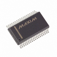
MAX6953EAX+ Maxim Integrated Products, MAX6953EAX+ Datasheet

MAX6953EAX+
Specifications of MAX6953EAX+
Related parts for MAX6953EAX+
MAX6953EAX+ Summary of contents
Page 1
... SET trademark of Philips Corp. SPI is a trademark of Motorola, Inc. ________________________________________________________________ Maxim Integrated Products For pricing, delivery, and ordering information, please contact Maxim/Dallas Direct! at 1-888-629-4642, or visit Maxim’s website at www.maxim-ic.com. Matrix LED Display Driver 400kbps 2-Wire Interface Compatible with I 7 dot-matrix LED 2 ...
Page 2
Interfaced, 2.7V to 5.5V, 4-Digit 5 Matrix LED Display Driver ABSOLUTE MAXIMUM RATINGS Voltage (with Respect to GND) V+ .............................................................................-0.3V to +6V All Other Pins................................................-0.3V to (V+ + 0.3V) O0–O13 Sink Current ....................................................... 500mA O14–O23 Source Current .................................................. 50mA ...
Page 3
Interfaced, 2.7V to 5.5V, 4-Digit 5 DC ELECTRICAL CHARACTERISTICS (continued) (Typical operating circuit 3.0V to 5.5V, T PARAMETER SYMBOL Segment Current Slew Rate Segment Drive Current Matching (Within IC) LOGIC INPUTS Input High Voltage SDA, SCL, AD0, ...
Page 4
Interfaced, 2.7V to 5.5V, 4-Digit 5 Matrix LED Display Driver MAX6953 TIMING CHARACTERISTICS (continued) (V+ = 2.7V to 5.5V unless otherwise noted.) (Note 1) A MIN MAX PARAMETER SYMBOL Fall Time of SDA ...
Page 5
Interfaced, 2.7V to 5.5V, 4-Digit 5 (Typical application circuit 3.3V, LED forward voltage = 2.4V, scan limit set to 4 digits, T DEAD CLOCK OSCILLATOR FREQUENCY vs. SUPPLY VOLTAGE 105 100 2.5 3.0 ...
Page 6
Interfaced, 2.7V to 5.5V, 4-Digit 5 Matrix LED Display Driver ISET PWM CURRENT BRIGHTNESS SOURCE CONTROL OSC ROW DIVIDER/ MULTIPLEXER COUNTER NETWORK CHARACTER CHARACTER GENERATOR GENERATOR RAM BLINK BLINK SPEED SELECT CONFIGURATION REGISTERS RAM SCL SDA SERIAL INTERFACE AD0 ...
Page 7
Interfaced, 2.7V to 5.5V, 4-Digit 5 One data bit is transferred during each clock pulse. The data on the SDA line must remain stable while SCL is high (Figure 4). The acknowledge bit is a clocked 9th bit that ...
Page 8
Interfaced, 2.7V to 5.5V, 4-Digit 5 Matrix LED Display Driver SDA SCL START CONDITION Figure 3. Start and Stop Conditions SDA SCL Figure 4. Bit Transfer SCL SDA BY TRANSMITTER SDA BY RECEIVER Figure 5. Acknowledge SDA 1 START ...
Page 9
Interfaced, 2.7V to 5.5V, 4-Digit 5 COMMAND BYTE IS STORED ON RECEIPT OF STOP CONDITION ACKNOWLEDGE FROM MAX6953 SLAVE ADDRESS S Figure 7. Command Byte Received HOW CONTROL BYTE AND DATA BYTE MAP INTO MAX6953's REGISTERS ACKNOWLEDGE FROM MAX6953 ...
Page 10
Interfaced, 2.7V to 5.5V, 4-Digit 5 Matrix LED Display Driver HOW COMMAND BYTE AND DATA BYTE MAP INTO MAX6953'S REGISTERS ACKNOWLEDGE FROM MAX6953 S SLAVE ADDRESS R/W Figure 9. n Data Bytes Received digit appears to flip between two ...
Page 11
Interfaced, 2.7V to 5.5V, 4-Digit 5 Table 4. Command Address Autoincrement Rules COMMAND BYTE ADDRESS RANGE x0000000 to x0000100 x0000101 x0000110 x000111 to x1111110 x1111111 Table 5. Register Address Map REGISTER No-Op Intensity10 Intensity32 Scan Limit Configuration User-Defined Fonts ...
Page 12
Interfaced, 2.7V to 5.5V, 4-Digit 5 Matrix LED Display Driver Table 6. Initial Power-Up Register Status REGISTER POWER-UP CONDITION Intensity10 1/16 (min on) Intensity32 1/16 (min on) Scan Limit Display 4 digits Shutdown enabled, blink ...
Page 13
Interfaced, 2.7V to 5.5V, 4-Digit 5 Table 10. Global Blink Enable/Disable (E Data Bit D3) Format MODE Blink function is disabled. Blink function is enabled. Table 11. Digit Register Mapping with Blink Globally Enabled SEGMENT’S SEGMENT’S BIT SETTING BIT ...
Page 14
Interfaced, 2.7V to 5.5V, 4-Digit 5 Matrix LED Display Driver Table 15. Character Map MSB x000 x001 x010 x011 x100 LSB 0000 RAM00 RAM16 0001 RAM01 RAM17 0010 RAM02 RAM18 0011 RAM03 RAM19 0100 RAM04 RAM20 0101 RAM05 RAM21 ...
Page 15
Interfaced, 2.7V to 5.5V, 4-Digit 5 Table 16. Memory Mapping of User-Defined Font Register 0x05 ADDRESS CODE REGISTER (HEX) DATA 0x05 0x00–0x7F 0x05 0x00–0x7F 0x05 0x80–0xFF Table 17. Font Pointer Address Behavior FONT POINTER ADDRESS 0x80 to 0xF6 0xF7 ...
Page 16
Interfaced, 2.7V to 5.5V, 4-Digit 5 Matrix LED Display Driver 100µs DIGIT 0 COLUMN DRIVER DIGIT 0 DIGIT 0 PINS O14-O18 ROW 2 ROW 3 ROW 1 COLUMN DRIVER DIGIT 1 DIGIT 1 DIGIT 1 ROW 2 PINS O19-O23 ...
Page 17
Interfaced, 2.7V to 5.5V, 4-Digit 5 Table 18. User-Definable Font Pointer Base Address Table FONT ADDRESS CHARACTER CODE (HEX) RAM00 0x05 RAM01 0x05 RAM02 0x05 RAM03 0x05 RAM04 0x05 RAM05 0x05 RAM06 0x05 RAM07 0x05 RAM08 0x05 RAM09 0x05 ...
Page 18
Interfaced, 2.7V to 5.5V, 4-Digit 5 Matrix LED Display Driver Table 19. User-Definable Character Storage Example FONT FONT ADDRESS ADDRESS CHARACTER CODE (HEX) POINTER RAM00 0x00 RAM00 0x01 RAM00 0x02 RAM00 0x03 RAM00 0x04 RAM01 0x05 RAM01 0x06 RAM01 ...
Page 19
Interfaced, 2.7V to 5.5V, 4-Digit 5 4MHz, which makes the blink frequencies 0.5Hz selec- table between 1Hz. The recommended value of R also sets the peak current to 40mA, which makes the segment current adjustable from 2.5mA to 37.5mA ...
Page 20
Interfaced, 2.7V to 5.5V, 4-Digit 5 Matrix LED Display Driver Table 23. Intensity Register Format for Digit 0 (Address 0x01) and Digit 2 (Address 0x02) TYPICAL DUTY SEGMENT CYCLE CURRENT (mA) 1/16 (min on) 2.5 2/16 5 3/16 7.5 ...
Page 21
Interfaced, 2.7V to 5.5V, 4-Digit 5 Low-Voltage Operation The MAX6953 works over the 2.7V to 5.5V supply range. The minimum useful supply voltage is deter- mined by the forward-voltage drop of the LEDs at the peak current I , ...
Page 22
Interfaced, 2.7V to 5.5V, 4-Digit 5 Matrix LED Display Driver TOP VIEW MAX6953 GND 4 GND 5 GND ...
Page 23
... Maxim cannot assume responsibility for use of any circuitry other than circuitry entirely embodied in a Maxim product. No circuit patent licenses are implied. Maxim reserves the right to change the circuitry and specifications without notice at any time. 23 ____________________Maxim Integrated Products, 120 San Gabriel Drive, Sunnyvale, CA 94086 408-737-7600 © 2004 Maxim Integrated Products Matrix LED Display Driver ...


