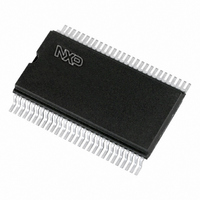
PCF8579T/1,112 NXP Semiconductors, PCF8579T/1,112 Datasheet - Page 13

PCF8579T/1,112
Manufacturer Part Number
PCF8579T/1,112
Description
IC LCD DRIVER DOT MATRIX 56-VSOP
Manufacturer
NXP Semiconductors
Datasheet
1.PCF8579T1112.pdf
(41 pages)
Specifications of PCF8579T/1,112
Package / Case
56-VSOP
Display Type
LCD
Configuration
Dot Matrix
Interface
I²C
Current - Supply
9µA
Voltage - Supply
2.5 V ~ 6 V
Operating Temperature
-40°C ~ 85°C
Mounting Type
Surface Mount
Maximum Clock Frequency
10 KHz
Operating Supply Voltage
2.5 V to 6 V
Maximum Power Dissipation
400 mW
Maximum Operating Temperature
+ 85 C
Maximum Supply Current
50 mA
Minimum Operating Temperature
- 40 C
Lead Free Status / RoHS Status
Lead free / RoHS Compliant
Digits Or Characters
-
Lead Free Status / Rohs Status
Lead free / RoHS Compliant
Other names
568-3562-5
935278869112
PCF8579TD
935278869112
PCF8579TD
NXP Semiconductors
PCF8579_5
Product data sheet
8.6.1 Bit transfer
8.6.2 START and STOP conditions
8.6.3 System configuration
8.6.4 Acknowledge
8.4 Timing generator
8.5 Column drivers
8.6 Characteristics of the I
The timing generator of the PCF8579 organizes the internal data flow from the RAM to the
display drivers. An external synchronization pulse SYNC is received from the PCF8578.
This signal maintains the correct timing relationship between cascaded devices.
Outputs C0 to C39 are column drivers which must be connected to the LCD. Unused
outputs should be left open-circuit.
The I
The two lines are a Serial Data Line (SDA) and a Serial Clock Line (SCL) which must be
connected to a positive supply via a pull-up resistor. Data transfer may be initiated only
when the bus is not busy.
One data bit is transferred during each clock pulse. The data on the SDA line must remain
stable during the HIGH period of the clock pulse as changes in the data line at this
moment will be interpreted as control signals.
Both data and clock lines remain HIGH when the bus is not busy. A HIGH-to-LOW
transition of the data line, while the clock is HIGH, is defined as the START condition (S).
A LOW-to-HIGH transition of the data line while the clock is HIGH, is defined as the STOP
condition (P).
A device transmitting a message is a transmitter, a device receiving a message is the
receiver. The device that controls the message flow is the master and the devices which
are controlled by the master are the slaves.
The number of data bytes transferred between the START and STOP conditions from
transmitter to receiver is unlimited. Each data byte of eight bits is followed by one
acknowledge bit. The acknowledge bit is a HIGH level put on the bus by the transmitter,
whereas the master generates an extra acknowledge related clock pulse. A slave receiver
which is addressed must generate an acknowledge after the reception of each byte. Also
a master must generate an acknowledge after the reception of each byte that has been
clocked out of the slave transmitter. The device that acknowledges must pull down the
SDA line during the acknowledge clock pulse, so that the SDA line is stable LOW during
the HIGH period of the acknowledge related clock pulse (set-up and hold times must be
taken into consideration). A master receiver must signal the end of a data transmission to
the transmitter by not generating an acknowledge on the last byte that has been clocked
out of the slave. In this event the transmitter must leave the data line HIGH to enable the
master to generate a STOP condition.
2
C-bus is for bidirectional, two-line communication between different ICs or modules.
Rev. 05 — 11 May 2009
2
C-bus
LCD column driver for dot matrix graphic displays
PCF8579
© NXP B.V. 2009. All rights reserved.
13 of 41


