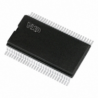
PCF8578T/1,112 NXP Semiconductors, PCF8578T/1,112 Datasheet - Page 9

PCF8578T/1,112
Manufacturer Part Number
PCF8578T/1,112
Description
IC LCD DRIVER DOT MATRIX 56-VSOP
Manufacturer
NXP Semiconductors
Specifications of PCF8578T/1,112
Package / Case
56-VSOP
Display Type
LCD
Configuration
Dot Matrix
Interface
I²C
Voltage - Supply
2.5 V ~ 6 V
Operating Temperature
-40°C ~ 85°C
Mounting Type
Surface Mount
Maximum Clock Frequency
3.3 KHz
Operating Supply Voltage
2.5 V to 6 V
Maximum Power Dissipation
400 mW
Maximum Operating Temperature
+ 150 C
Maximum Supply Current
50 mA
Minimum Operating Temperature
- 65 C
Lead Free Status / RoHS Status
Lead free / RoHS Compliant
Current - Supply
-
Digits Or Characters
-
Lead Free Status / Rohs Status
Details
Other names
568-3561-5
935278868112
PCF8578TD
935278868112
PCF8578TD
Philips Semiconductors
7.3
The bias levels required to produce maximum contrast
depend on the multiplex rate and the LCD threshold
voltage (V
which the LCD exhibits 10% contrast. Table 2 shows the
optimum voltage bias levels for the PCF8578 as functions
of V
ratios (D) for the different multiplex rates. A practical value
for V
shows the first 4 rows of Table 2 as graphs. Table 3 shows
the relative values of the resistors required in the
configuration of Fig.5 to produce the standard multiplex
rates.
Table 2 Optimum LCD voltages
Table 3 Multiplex rates and resistor values for Fig.5
2003 Apr 14
-------- -
V
-------- -
V
-------- -
V
-------- -
V
V
-------- -
V
--------------------- -
V
-------------------- -
D
V
RESISTORS
V
V
V
V
PARAMETER
LCD row/column driver for
dot matrix graphic displays
op
op
op
op
op
th
off rms
on rms
2
3
4
5
V
op
V
=
op
op
op
(V
R1
R2
R3
--------------------- -
V
V
Multiplexed LCD bias generation
is obtained by equating V
on rms
off rms
op
th
= V
). V
DD
th
is typically defined as the RMS voltage at
V
0.739
0.522
0.478
0.261
0.297
0.430
1.447
3.370
1 : 8
LCD
3
n = 8
n 2
–
), together with the discrimination
MULTIPLEX RATE (n)
R
–
n
MULTIPLEX RATE
R
R
1 : 16
0.800
0.600
0.400
0.200
0.245
0.316
1.291
4.080
off(rms)
with V
1 : 24
0.830
0.661
0.339
0.170
0.214
0.263
1.230
4.680
n = 16, 24, 32
n 3
th
R
R
–
. Figure 4
1 : 32
0.850
0.700
0.300
0.150
0.193
0.230
1.196
5.190
R
9
7.4
At power-on the PCF8578 resets to a defined starting
condition as follows:
1. Display blank
2. 1 : 32 multiplex rate, row mode
3. Start bank, 0 selected
4. Data pointer is set to X, Y address 0, 0
5. Character mode
6. Subaddress counter is set to 0
7. I
Data transfers on the I
following power-on, to allow completion of the reset action.
V
Fig.4
V bias
V op
bias
2
C-bus interface is initialized.
Power-on reset
= V
1.0
0.8
0.6
0.4
0.2
2
0
, V
V
3
bias
, V
4
, V
/V
5
op
. See Table 2.
1:8
as a function of the multiplex rate.
2
C-bus should be avoided for 1 ms
1:16
V 2
V 3
V 4
V 5
Product specification
1:24
multiplex rate
PCF8578
MSA838
1:32


