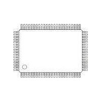
PCA8534AH/Q900/1,5 NXP Semiconductors, PCA8534AH/Q900/1,5 Datasheet - Page 22

PCA8534AH/Q900/1,5
Manufacturer Part Number
PCA8534AH/Q900/1,5
Description
IC LCD DRIVER 60SEG 80LQFP
Manufacturer
NXP Semiconductors
Datasheet
1.PCA8534AHQ90015.pdf
(44 pages)
Specifications of PCA8534AH/Q900/1,5
Package / Case
80-LQFP
Display Type
LCD
Configuration
60 Segment
Interface
I²C
Current - Supply
80µA
Voltage - Supply
1.8 V ~ 5.5 V
Operating Temperature
-40°C ~ 85°C
Mounting Type
Surface Mount
Number Of Digits
30
Number Of Segments
60
Maximum Clock Frequency
3046 Hz
Operating Supply Voltage
1.8 V to 5.5 V
Maximum Power Dissipation
400 mW
Maximum Operating Temperature
+ 95 C
Attached Touch Screen
No
Maximum Supply Current
20 uA
Minimum Operating Temperature
- 40 C
Lead Free Status / RoHS Status
Lead free / RoHS Compliant
Digits Or Characters
-
Lead Free Status / Rohs Status
Details
Other names
568-5110-2
Available stocks
Company
Part Number
Manufacturer
Quantity
Price
Company:
Part Number:
PCA8534AH/Q900/1,5
Manufacturer:
NXP Semiconductors
Quantity:
10 000
NXP Semiconductors
PCA8534A_2
Product data sheet
Fig 15. I
EXAMPLES
a) transmit two bytes of RAM data
b) transmit two command bytes
c) transmit one command byte and two RAM date bytes
S 0 1 1 1 0
S 0 1 1 1 0
S 0 1 1 1 0
S 0 1 1 1 0
2
slave address
C-bus protocol
0
0
0
0
R/W = 0
S
A
0
S
A
0
S
A
0
S
A
0
0
0
0
0
The PCA8534A is a write-only device and will not respond to a read access, therefore bit
0 should always be logic 0. Bit 1 of the slave address byte that a PCA8534A will respond
to, is defined by the level tied to its SA0 input (V
Having two reserved slave addresses allows the following on the same I
The I
condition (S) from the I
slave addresses available. All PCA8534A whose SA0 inputs correspond to bit 0 of the
slave address respond by asserting an acknowledge in parallel. This I
ignored by all PCA8534A whose SA0 inputs are set to the alternative level.
After an acknowledgement, one or more command bytes follow that define the status of
each addressed PCA8534A.
The last command byte sent is identified by resetting its most significant bit, continuation
bit CO (see
PCA8534A on the bus.
A
A
A
A
Fig 16. Control byte format
•
•
C
O
0 1
1 0
1 0
R
Up to 16 PCA8534A for very large LCD applications
The use of two types of LCD multiplex drive
S
2
control byte
C-bus protocol is shown in
Figure
All information provided in this document is subject to legal disclaimers.
A
A
A
A
M
S
B
RAM/command byte
16). The command bytes are also acknowledged by all addressed
COMMAND
COMMAND
RAM DATA
2
C-bus master which is followed by one of two possible PCA8534A
Rev. 02 — 1 June 2010
MSB
S
B
L
CO
7
P
A
A
A
Figure
0 0
0 1
RS
6
RAM DATA
5
15. The sequence is initiated with a START
Universal LCD driver for low multiplex rates
4
not relevant
3
A
A
A
SS
P
2
for logic 0 and V
COMMAND
RAM DATA
1
mgl753
0
LSB
A
A
P
PCA8534A
DD
RAM DATA
2
for logic 1).
C-bus transfer is
© NXP B.V. 2010. All rights reserved.
2
C-bus:
mgl752
A
P
22 of 44


