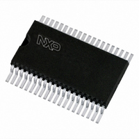
PCF8577CT/3,118 NXP Semiconductors, PCF8577CT/3,118 Datasheet - Page 8

PCF8577CT/3,118
Manufacturer Part Number
PCF8577CT/3,118
Description
IC LCD DRIVER 32/64SEG 40-VSOP
Manufacturer
NXP Semiconductors
Datasheet
1.PCF8577CT3118.pdf
(28 pages)
Specifications of PCF8577CT/3,118
Package / Case
40-VSOP
Display Type
LCD
Configuration
32 Segment
Interface
I²C
Voltage - Supply
2.5 V ~ 6 V
Operating Temperature
-40°C ~ 85°C
Mounting Type
Surface Mount
Number Of Digits
32
Number Of Segments
64
Maximum Clock Frequency
100 KHz
Operating Supply Voltage
2.5 V to 6 V
Maximum Power Dissipation
500 mW
Maximum Operating Temperature
+ 85 C
Maximum Supply Current
125 uA
Minimum Operating Temperature
- 40 C
Lead Free Status / RoHS Status
Lead free / RoHS Compliant
Current - Supply
-
Digits Or Characters
-
Lead Free Status / Rohs Status
Lead free / RoHS Compliant
Other names
568-1082-2
935278866118
PCF8577CTD-T
935278866118
PCF8577CTD-T
Available stocks
Company
Part Number
Manufacturer
Quantity
Price
Part Number:
PCF8577CT/3,118
Manufacturer:
NXP/恩智浦
Quantity:
20 000
Philips Semiconductors
6.7
At power-on reset the PCF8577C resets to a defined
starting condition as follows:
1. Both backplane outputs are set to V
2. All segment outputs are set to V
3. The segment byte registers and control register are
4. The I
6.8
The PCF8577C slave address is shown in Fig.6.
Before any data is transmitted on the I
which should respond is addressed first. The addressing is
always done with the first byte transmitted after the start
procedure.
1998 Jul 30
LCD direct/duplex driver with
I
2
to 3-state in cascade mode
cleared
C-bus interface
Power-on reset
Slave address
2
C-bus interface is initialized.
Fig.6 PCF8577C slave address.
S
MGA732
0 1 1 1 0 1 0 0
SLAVE ADDRESS
S
SLAVE ADDRESS
SS
MGA731
2
SS
acknowledge by
C-bus, the device
all PCF8577C
A
R/W
in master mode;
0
A
Fig.7 I
control byte
BYTE VECTOR
SEGMENT
2
C-bus protocol.
8
acknowledge by
6.9
The PCF8577C I
The PCF8577C is a slave receiver and has a fixed slave
address (see Fig.6). All PCF8577Cs with the same slave
address acknowledge the slave address in parallel.
The second byte is always the control byte and is loaded
into the control register of each PCF8577C connected to
the I
control byte. Subsequent data bytes are loaded into the
segment registers of the selected device. Any number of
data bytes may be loaded in one transfer and in an
expanded system rollover of the SBV from 111 111 to
000 000 is allowed. If a stop (P) condition is given after the
control byte acknowledge the segment data will remain
unchanged. This allows the BANK bit to be toggled without
changing the segment register contents. During loading of
segment data only the selected PCF8577C gives an
acknowledge. Loading is terminated by generating a stop
(P) condition.
all PCF8577C
2
A
C-bus. All addressed devices acknowledge the
msb
I
2
C-bus protocol
SEGMENT DATA
n bytes
2
C-bus protocol is shown in Fig.7.
selected PCF8577C only
acknowledge by
segment byte vector
auto increment
lsb
A
P
Product specification
PCF8577C


