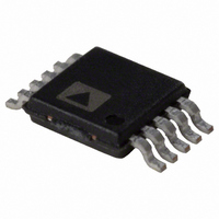
AD8213YRMZ Analog Devices Inc, AD8213YRMZ Datasheet

AD8213YRMZ
Specifications of AD8213YRMZ
Available stocks
Related parts for AD8213YRMZ
AD8213YRMZ Summary of contents
Page 1
FEATURES ±4000 V HBM ESD High common-mode voltage range − +65 V operating − +68 V survival Buffered output voltage Wide operating temperature range 10-lead MSOP: −40°C to +125°C Excellent ac and dc performance 3 μV/°C ...
Page 2
AD8213 TABLE OF CONTENTS Features .............................................................................................. 1 Applications ....................................................................................... 1 Functional Block Diagram .............................................................. 1 General Description ......................................................................... 1 Revision History ............................................................................... 2 Specifications ..................................................................................... 3 Absolute Maximum Ratings ............................................................ 4 ESD Caution .................................................................................. 4 Pin Configuration and Function Descriptions ...
Page 3
SPECIFICATIONS T = operating temperature range, V OPR S Table 1. Parameter GAIN Initial Accuracy Accuracy Over Temperature Gain vs. Temperature VOLTAGE OFFSET Offset Voltage (RTI) Over Temperature (RTI) Offset Drift INPUT Input Impedance Differential Common Mode Common-Mode Input Voltage ...
Page 4
AD8213 ABSOLUTE MAXIMUM RATINGS Table 2. Parameter Supply Voltage Continuous Input Voltage Reverse Supply Voltage HBM (Human Body Model) ESD Rating CDM (Charged Device Model) ESD Rating Operating Temperature Range Storage Temperature Range Output Short-Circuit Duration Stresses above those listed ...
Page 5
PIN CONFIGURATION AND FUNCTION DESCRIPTIONS Figure 2. Metallization Diagram Table 3. Pin Function Descriptions Pin No. Mnemonic X 1 −IN2 −401 2 +IN2 −401 3 GND −401 4 OUT2 −394 ...
Page 6
AD8213 TYPICAL PERFORMANCE CHARACTERISTICS 0.8 0.7 0.6 0.5 0.4 0.3 0.2 0.1 0 –0.1 –0.2 –0.3 –0.4 –0.5 –0.6 –0.7 –0.8 –40 – TEMPERATURE (°C) Figure 4. Typical Offset Drift 130 COMMON-MODE VOLTAGE > 5V 120 ...
Page 7
INPUT COMMON-MODE VOLTAGE (V) Figure 10. Input Bias Current vs. Common-Mode Voltage (Per Input) 7.0 6.5 6.0 5.5 5.0 4.5 4.0 3.5 3.0 2.5 2.0 1.5 ...
Page 8
AD8213 2V/DIV 0.01/DIV TIME (5µs/DIV) Figure 16. Settling Time (Falling) 2V/DIV 0.01/DIV TIME (5µs/DIV) Figure 17. Settling Time (Rising –40 – TEMPERATURE (°C) ...
Page 9
V (µV/°C) OS Figure 22. Offset Drift Distribution (μV/°C) (Temperature Range = −40°C to +125°C) 1400 1200 1000 800 600 400 200 0 –24 –21 –18 –15 –12 –9 ...
Page 10
AD8213 THEORY OF OPERATION In typical applications, the AD8213 amplifies a small differential input voltage generated by the load current flowing through a shunt resistor. The AD8213 rejects high common-mode voltages ( and provides a ground referenced, ...
Page 11
APPLICATION NOTES OUTPUT LINEARITY In all current sensing applications, and especially in automotive and industrial environments where the common-mode voltage can vary significantly important that the current sensor maintain the specified output linearity, regardless of the input differential ...
Page 12
AD8213 APPLICATIONS INFORMATION HIGH-SIDE CURRENT SENSE WITH A LOW-SIDE SWITCH In such load control configurations, the PWM controlled switch is ground referenced. An inductive load (solenoid) is tied to a power supply. A resistive shunt is placed between the switch ...
Page 13
BIDIRECTIONAL CURRENT SENSING The AD8213 can also be configured to sense current in both directions at the inputs. This configuration is useful in charge/ discharge applications. A typical connection diagram is shown in Figure 31. In this mode Channel 1 ...
Page 14
... AD8213 OUTLINE DIMENSIONS ORDERING GUIDE Model Temperature Range 1 AD8213YRMZ −40°C to +125°C 1 AD8213YRMZ-RL −40°C to +125°C 1 AD8213YRMZ-RL7 −40°C to +125°C 1 AD8213WYRMZ −40°C to +125°C 1 AD8213WYRMZ-RL −40°C to +125°C 1 AD8213WYRMZ-R7 −40°C to +125° RoHS Compliant Part. ...
Page 15
NOTES Rev Page AD8213 ...
Page 16
AD8213 NOTES ©2007–2009 Analog Devices, Inc. All rights reserved. Trademarks and registered trademarks are the property of their respective owners. D06639-0-5/09(A) Rev Page ...


