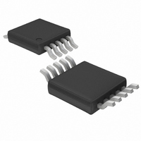
LTC4151IMS#PBF Linear Technology, LTC4151IMS#PBF Datasheet - Page 11

LTC4151IMS#PBF
Manufacturer Part Number
LTC4151IMS#PBF
Description
IC CURRENT MONITOR(12BIT) 10MSOP
Manufacturer
Linear Technology
Specifications of LTC4151IMS#PBF
Function
Current Monitor (12 Bit)
Sensing Method
High-Side
Accuracy
±1%
Voltage - Input
7 ~ 80 V
Operating Temperature
-40°C ~ 85°C
Mounting Type
Surface Mount
Package / Case
10-MSOP, Micro10™, 10-uMAX, 10-uSOP
Voltage Supervisor Type
Voltage Monitor
Number Of Voltage Supervisors
1
Reset Threshold Voltage (min)
2.3V
Reset Threshold Voltage (max)
2.9V
Operating Supply Voltage (min)
7V
Operating Supply Voltage (max)
80V
Package Type
MSOP
Operating Temperature Classification
Industrial
Operating Temp Range
-40C to 85C
Pin Count
10
Mounting
Surface Mount
Lead Free Status / RoHS Status
Lead free / RoHS Compliant
Current - Output
-
Lead Free Status / Rohs Status
Compliant
Available stocks
Company
Part Number
Manufacturer
Quantity
Price
Table 1. LTC4151 Device Addressing*
*H = Tie High; L = Tie to GND; NC = Open; X = Don’t Care
I
Nine distinct I
three-state pins ADR0 and ADR1, as shown in Table 1.
Address bits a6, a5 and a4 are configured to (110) and
the least significant bit is the R/W bit. In addition, the
LTC4151 will respond to a mass write address (1100 110)b
for writing to all LTC4151s, regardless of their individual
address settings.
Acknowledge
The acknowledge signal is used for handshaking between
the transmitter and the receiver to indicate that the last
byte of data was received. The transmitter always releases
the SDA line during the acknowledge clock pulse. The
LTC4151 pulls the SDA line low on the 9th clock cycle to
acknowledge receipt of the data. If the slave fails to ac-
knowledge by leaving SDA high, then the master can abort
the transmission by generating a Stop condition. When
the master is receiving data from the slave, the master
must pull down the SDA line during the clock pulse to
indicate receipt of a data byte, and that another byte is to
be read. After the last byte has been received the master
will leave the SDA line high (not acknowledge) and issue
a Stop condition to terminate the transmission.
Write Protocol
The master begins a write operation with a Start condition
followed by the seven bit slave address and the R/W bit
APPLICATIONS INFORMATION
2
C Device Addressing
DESCRIPTION
Mass Write
0
1
2
3
4
5
6
7
8
2
C bus addresses are configurable using the
HEX DEVICE
ADDRESS
CC
D0
D2
D4
D6
D8
DA
DC
DE
CE
h
a6
1
1
1
1
1
1
1
1
1
1
a5
1
1
1
1
1
1
1
1
1
1
a4
0
0
0
0
0
0
0
0
0
0
BINARY DEVICE ADDRESS
a3
0
0
1
1
1
1
1
1
1
1
set to zero. After the addressed LTC4151 acknowledges
the address byte, the master then sends a command
byte which indicates which internal register the master
wishes to write. The LTC4151 acknowledges this and
then latches the lower three bits of the command byte
into its internal register address pointer. The master then
delivers the data byte and the LTC4151 acknowledges
once more and latches the data into its internal register.
If the master continues sending a second byte or more
data bytes, as in a Write Word or Write Page command,
the second byte or more data bytes will be acknowledged
by the LTC4151, the internal register address pointer
will increment automatically, and each byte of data will
be latched into an internal register corresponding to the
address pointer. The write operation terminates and the
register address pointer resets to 00h when the master
sends a Stop condition.
Read Protocol
The master begins a read operation with a Start condition
followed by the seven bit slave address and the R/W bit
set to zero. After the addressed LTC4151 acknowledges
the address byte, the master then sends a command
byte that indicates which internal register the master
wishes to read. The LTC4151 acknowledges this and then
latches the lower three bits of the command byte into its
internal register address pointer. The master then sends
a repeated Start condition followed by the same seven bit
a2
1
1
0
0
0
0
1
1
1
1
a1
1
1
1
0
0
1
1
0
0
1
a0
0
1
0
1
0
1
0
1
0
1
R/W
X
0
X
X
X
X
X
X
X
X
LTC4151
ADR1
ADDRESS PINS
NC
NC
NC
X
H
H
H
L
L
L
LTC4151
11
ADR0
NC
NC
NC
H
H
H
X
L
L
L
4151fc


