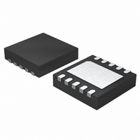
LTC4151IDD#TRPBF Linear Technology, LTC4151IDD#TRPBF Datasheet - Page 6

LTC4151IDD#TRPBF
Manufacturer Part Number
LTC4151IDD#TRPBF
Description
IC CURRENT MONITOR(12BIT) 10DFN
Manufacturer
Linear Technology
Datasheet
1.LTC4151CMS-1PBF.pdf
(18 pages)
Specifications of LTC4151IDD#TRPBF
Function
Current Monitor (12 Bit)
Sensing Method
High-Side
Accuracy
±1%
Voltage - Input
7 ~ 80 V
Operating Temperature
-40°C ~ 85°C
Mounting Type
Surface Mount
Package / Case
10-DFN
Lead Free Status / RoHS Status
Lead free / RoHS Compliant
Current - Output
-
Available stocks
Company
Part Number
Manufacturer
Quantity
Price
LTC4151
TYPICAL PERFORMANCE CHARACTERISTICS
PIN FUNCTIONS
ADIN: ADC Input. The onboard ADC measures voltage
range between 0V and 2.048V. Tie to GND if unused.
ADR1, ADR0: I
ADR1 and ADR0 to V
configures one of nine possible addresses. See Table 1
in the Applications Information section for details.
Exposed Pad (DD Package Only): Exposed pad may be
left open or connected to device ground (GND).
GND: Device Ground.
SCL: I
the SDA pin on rising edges of SCL. This pin is driven
by an open-collector output from a master controller. An
external pull-up resistor or current source is required and
can be placed between SCL and V
is internally clamped to 6V (5.5V minimum).
SDA (LTC4151 Only): I
shifting in address, command or data bits and sending
out data. An external pull-up resistor or current source
is required and can be placed between SDA and V
The voltage at SDA is internally clamped to 6V (5.5V
minimum).
SDAI (LTC4151-1/LTC4151-2 Only): I
Used for shifting in address, command, data, and SDAO
acknowledge bits. This pin is driven by an open-collector
6
2
C Bus Clock Input. Data is shifted in and out at
0.5
0.4
0.3
0.2
0.1
2
0
C Device Address Inputs. Connecting
0
SDA, SDAO, SDAO Output Low vs
Pull-Up Current (V
2
IN
C Bus Data Input/Output. Used for
, GND or leaving the pins open
5
I
SDA
10
(mA)
SDA(OL)
IN
. The voltage at SCL
2
C Bus Data Input.
15
vs I
– 40°C
SDA
4151 G09
85°C
25°C
)
20
IN
.
output from a master controller. An external pull-up resistor
or current source is required and can be placed between
SDAI and V
data read at SDAO needs to be echoed back to SDAI for
proper I
clamped to 6V (5.5V minimum).
SDAO (LTC4151-2 Only): Serial Bus Data Output. Open-
drain output used for sending data back to the master
controller or acknowledging a write operation. Normally
tied to SDAI to form the SDA line. An external pull-up
resistor or current source is required.
SDAO (LTC4151-1 Only): Inverted Serial Bus Data Out-
put. Open-drain output used for sending data back to the
master controller or acknowledging a write operation. Data
is inverted for convenience of opto-isolation. An external
pull-up resistor or current source is required.
SENSE
recommended Kelvin connection.
SENSE
external sense resistor between SENSE
The differential voltage between SENSE
monitored by the onboard ADC with a full-scale sense
voltage of 81.92mV.
6.1
6.0
5.9
6.3
6.2
+
–
0.01
2
: Kelvin Sense of the V
: High Side Current Sense Input. Connect an
C communication. The voltage at SDAI is internally
SDA, SDAI, SCL Clamp Voltage
vs Load Current
– 40°C
85°C
V
IN
IN
. If the master separates SDAI and SDAO,
= 12V, T
25°C
0.1
I
LOAD
A
= 25°C, unless noted.
(mA)
1
IN
Pin. See Figure 10 for
4151 G10
10
+
+
and SENSE
and SENSE
4151fc
–
–
is
.


