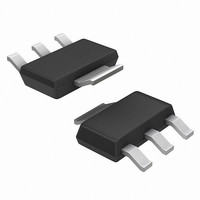
NCP1011ST130T3G ON Semiconductor, NCP1011ST130T3G Datasheet - Page 10

NCP1011ST130T3G
Manufacturer Part Number
NCP1011ST130T3G
Description
IC CTRLR/MOSFET 130KHZ SOT223
Manufacturer
ON Semiconductor
Datasheet
1.NCP1010ST100T3G.pdf
(24 pages)
Specifications of NCP1011ST130T3G
Output Isolation
Isolated
Frequency Range
117 ~ 143kHz
Voltage - Input
8.5 ~ 10 V
Voltage - Output
700V
Power (watts)
19W
Operating Temperature
-40°C ~ 125°C
Package / Case
TO-261-4, TO-261AA, SOT-223-4
Duty Cycle (max)
72 %
Mounting Style
SMD/SMT
Switching Frequency
143 KHz
Operating Supply Voltage
- 0.3 V to + 10 V
Maximum Operating Temperature
+ 150 C
Synchronous Pin
No
Topology
Flyback
Lead Free Status / RoHS Status
Lead free / RoHS Compliant
Other names
NCP1011ST130T3G
NCP1011ST130T3GOSTR
NCP1011ST130T3GOSTR
Available stocks
Company
Part Number
Manufacturer
Quantity
Price
Company:
Part Number:
NCP1011ST130T3G
Manufacturer:
ON Semiconductor
Quantity:
500
Part Number:
NCP1011ST130T3G
Manufacturer:
ON/安森美
Quantity:
20 000
is expressed by:
the IC actually pulses is given by
Finally,
using the same formula topology:
From these three definitions, the burst duty- -cycle
can be computed:
equation with values extracted from the parameter section
gives a typical duty- -cycle of 13%, precluding any lethal
thermal runaway while in a fault condition.
DSS Internal Dissipation
drain pin. In Flyback- -based converters, this drain level can
easily go above 600 V peak and thus increase the stress on the
DSS startup source. However, the drain voltage evolves with
time and its period is small compared to that of the DSS. As
a result, the averaged dissipation, excluding capacitive losses,
can be derived by:
Figure 17 portrays a typical drain- -ground waveshape where
leakage effects have been removed.
dc =
The rising slope from the latch- -off level up to 8.5 V
The Dynamic Self- -Supplied pulls energy out from the
ICC1 ·
the
ICC1
ΔV2
ΔV2
Tstart =
latch- -off
+
P DSS = ICC1 · < Vds(t) > .
ΔV1
IC1
dc =
+
ΔV1 · C
ICC2
Tstart + Tsw + TLatch
ΔV3
IC1
Figure 16. NCP101X Facing a Fault Condition (Vin = 150 Vdc)
time
Tstart
(eq. 3)
. The time during which
Tsw
can
TLatch =
.
Tsw
tsw =
Feeding
be
ΔV3 · C
ΔV2 · C
derived
ICC2
ICC1
(eq. 2)
(eq. 4)
http://onsemi.com
the
TLatch
.
.
.
.
10
derived by additive square area calculation:
toff can be expressed by:
can be evaluated by:
1 V Ripple
By looking at Figure 17, the average result can easily be
By developing Equation 5, we obtain:
Vds(t)
Figure 17. A typical drain- -ground waveshape
where leakage effects are not accounted for.
Latch--off
< Vds(t) >= Vin − Vin · ton
Vin
Level
< Vds(t) >= Vin · (1 − d) + Vr · toff
ton
Vr
Tsw
ton = Ip ·
toff
toff = Ip ·
dt
Vin
Lp
Tsw
(eq. 8)
Lp
Vr
+ Vr · toff
(eq. 7)
.
Tsw
Tsw
where ton
(eq. 5)
(eq. 6)
t


