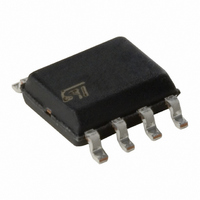
L6565DTR STMicroelectronics, L6565DTR Datasheet - Page 4

L6565DTR
Manufacturer Part Number
L6565DTR
Description
IC CTCLR PWM SMPS CM UVLO 8SOIC
Manufacturer
STMicroelectronics
Datasheet
1.L6565DTR.pdf
(17 pages)
Specifications of L6565DTR
Mfg Application Notes
25W Converter Using the L6565 AppNote 30 W Adapter with PWM L6565 Controller AppNote 80 W SMPS - L6565/ESBT STC04IE170HV AppNote L6565 Quasi-Resonant Controller AppNote L6565-Based Low Cost SMPS for TV AppNote SMPS for CRT Monitors with the L6565 AppNote STEVAL-TSP001V1 AppNote Wide Input Volt Range SMPS for Metering AppNote
Output Isolation
Isolated
Voltage - Input
10.3 ~ 18 V
Power (watts)
650mW
Operating Temperature
-40°C ~ 150°C
Package / Case
8-SOIC (0.154", 3.90mm Width)
Operating Temperature Range
- 40 C to + 150 C
Mounting Style
SMD/SMT
For Use With
497-9051 - BOARD DEMO STC03DE220HV/ L6565497-8410 - BOARD EVAL STP12IE95F4497-8227 - BOARD EVAL L6565/STW3N150497-6427 - BOARD EVAL POE STHS4257A/L6565D497-6422 - BOARD EVAL BASED ON L6565497-6415 - BOARD EVAL L6565/STW4N150 BASED497-6414 - BOARD EVAL L6565 EU220V BASED497-6339 - BOARD EVAL SMPS L6565 3PHASE APP497-6255 - BOARD 6W 3PH SMPS METERING ESBT497-5680 - POWER SUPPLY FOR STB US-110V497-5679 - BOARD EVAL 3PHASE W/ESBT 100W
Lead Free Status / RoHS Status
Lead free / RoHS Compliant
Other names
497-4017-2
497-4017-2
497-4584-2
E-L6565DTR
497-4017-2
497-4584-2
E-L6565DTR
Available stocks
Company
Part Number
Manufacturer
Quantity
Price
Part Number:
L6565DTR
Manufacturer:
ST
Quantity:
20 000
L6565
ELECTRICAL CHARACTERISTCS (continued)
(T
4/17
CURRENT SENSE COMPARATOR
ZERO CURRENT DETECTOR/ SYNCHRONIZATION
START TIMER
GATE DRIVER
Symbol
I
T
I
V
V
V
V
V
V
ZCDsnk
j
ZCDsrc
I
I
t
t
I
BLANK
I
START
COMP
V
ZCDb
V
d(H-L)
= -25 to 125°C, V
ZCDH
ZCDr
V
GDoff
COMP
CSdis
ZCDL
ZCDA
ZCDT
V
GB
I
G
CS
CSx
DIS
OH
t
t
OL
f
r
V
(1) Parameters guaranteed by design, not tested in production.
Voltage Gain
Gain-Bandwidth Product
Source Current
Sink Current
Upper Clamp Voltage
Lower Clamp Voltage
Input Bias Current
Delay to Output
Current Sense Reference Clamp
Hiccup-mode OCP level
Upper Clamp Voltage
Lower Clamp Voltage
Arming Voltage
(positive-going edge)
Triggering Voltage
(negative-going edge)
Input Bias Current
Source Current Capability
Sink Current Capability
Disable Threshold
Restart Current After Disable
Blanking time after pin 7 high-to-
low transition
Start Timer period
Dropout Voltage
Current Fall Time
Current Rise Time
I
GD
sink current
CC
Parameter
= 12V, C
o
= 1nF; unless otherwise specified)
Open loop
V
V
I
I
V
V
V
V
I
I
(1)
V
V
V
V
I
I
I
I
Vcc = 4 V, V
SOURCE
SINK
ZCD
ZCD
GDsource
GDsource
GDsink
GDsink
COMP
COMP
COMP
COMP
COMP
CS
ZCD
ZCD
COMP
COMP
= 0
= 3mA
= - 3mA
= 0.5 mA
= 1 to 4.5 V
< V
= Upper clamp, V
= Upper clamp, V
= 200mA
= 20mA
= Upper clamp, V
= 4V, V
= 4V, V
= 2.5 V
Test Condition
= 200mA
= 20mA
DIS
= 0.5 mA
3.2 V
GD
, Vcc > Vcc
INV
INV
= 1 V
= 2.4 V
= 2.6 V
VFF
VFF
VFF
off
= 1.5V
= 0V
= 3V
Min.
1.28
0.62
1.85
150
250
2.5
4.7
0.3
-70
60
-2
-3
5
3
5
-0.05
Typ.
2.25
0.65
-150
-3.5
200
200
400
4.5
5.5
1.4
0.7
2.0
5.2
2.1
1.6
3.5
1.2
0.7
80
18
40
40
10
1
0
2
Max.
2.55
0.78
-230
450
250
550
100
100
1.5
0.2
2.2
6.1
-10
0.3
10
-5
-1
1
2
1
2
MHz
Unit
mA
mA
mA
mA
mV
mA
dB
µA
µA
µA
ns
µs
µs
ns
ns
V
V
V
V
V
V
V
V
V
V


